Tx, rx and oe paths in data bits – Achronix Speedster22i Memory PHY User Manual
Page 14
14
UG043, April 26, 2014
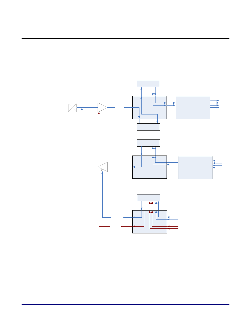
TX, RX and OE paths in Data Bits
This section highlights the pieces of the TX, RX and OE circuitry that make up each of the
data bits. These same pieces are also used in building clock, dqs and dm bits also, and the
flexibility provided enables more custom IO configurations to be created as well. Figure 8
shows a block level diagram of the TX, RX and OE paths. The paths and the modules used
are described in more detail below.
DQ PAD
rx_any
ipbit_y
sdll
rx_fifo
rx_sd
tx_any
opbit_data_out
tx_flop
tx_sd
oeren_any
opbit_oe
oeren_flop
opbit_rtt
Figure 8: TX, RX and OE paths in a DDR DQ bit
Receive path: Data coming from the DQ pad goes through the receive buffer and is then
provided as an input to the rx_any module. This data then goes through a slave dll (sdll)
which is essentially used to implement read-leveling. The output of the sdll is then fed into
the rx_fifo module which contains a fifo of depth four (at full-rate). At this point, the receive
data is sampled at the positive and negative edges for full-rate conversion, and a clock
domain transfer take place in the fifo between the dqs clock domain and the full-rate clock
domain coming from the FPGA PLL. The output of the rx_fifo is then optionally fed into a
rx_sd module which implements a full-rate to half-rate conversion prior to transferring the
four-wide data into the fabric.