Dqs clocking and circuitry, Read path write path – Achronix Speedster22i Memory PHY User Manual
Page 16

16
UG043, April 26, 2014
DQS Clocking and Circuitry
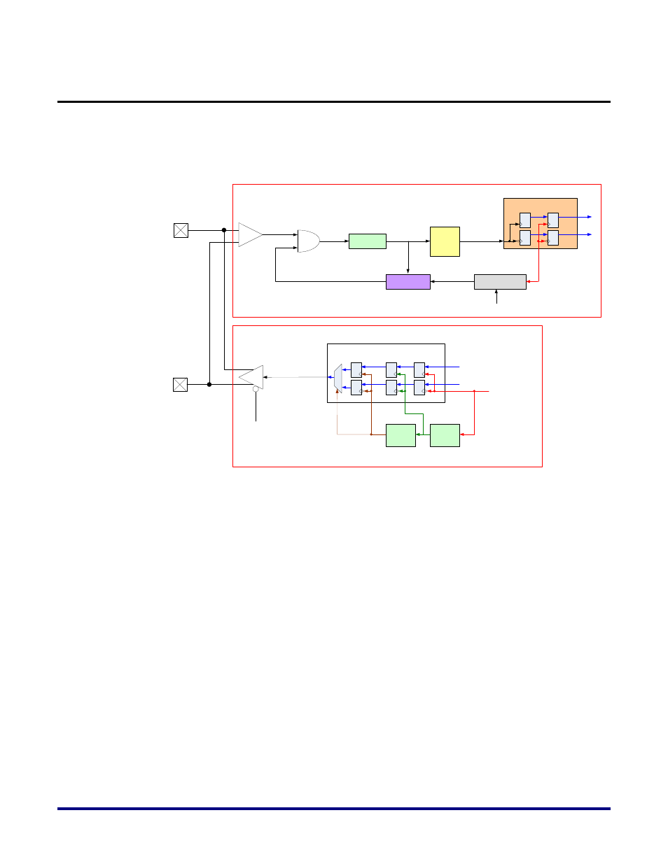
The circuitry in Figure 9 below shows how the DQS signal coming from or going to
dqsn/dqsp is treated to ensure that both reads and writes can be successfully done for high
data rate DDR3 implementations.
DQSP PAD
DQSN PAD
OE
DLL
Clock
Mux
Rx_FIFO in dq_bits
dataa
datab
dqs_rx_fifo_clk
Full-rate fabric
clock from PLL
Postamble
dqs_clkout
postamble_out
ddr3_dq9_bit
wpb_preamb_en
phy_ctrli_dqa/b9
TX_Flop
DLL
(0.75T)
DLL
(0.25T)
phy_ctrli_dqsa
1'b0
Full-rate fabric clock
from PLL
Write-leveling
implementation in TX Flop
Read Path
Write Path
Figure 9: DQS Circuitry for Read and Write
For the read path, the dqs signal goes through a gate that acts to control the preamble enable
and the postamble shutoff. This control logic is provided through input signals
phy_ctrli_dqa/b9 that first traverse some logic in the ddr3_dq9_bit module. This is done to
ensure that gating logic coming in has a delay that matches the dq signal delay through a
ddr3_dq{1-8}_bit. The DLL delayed dqs_clkout signal and the preamble signal from the
ddr3_dq9_bit are used to generate the final postamble_out signal that is then fed into the gate
controlling the dqs signal coming in, ultimately creating a feedback path through a DLL
which ensures that PVT compensation is done appropriately. The section below on DLL
Specs and Operation provides more details on the specifics of the DLL. The dqs_clkout signal
from the DLL feeds a clk mux which is then distributed to the rx_fifo modules of all of the dq
bits that this dqs signal needs to sample. The dqs signal is used as a clock for the first fifo
stage, and the second register stage in the fifo is clocked by a full-rate clock provided by a
PLL in the FPGA to ensure that data beyond this fifo is synchronized to a core clock for all
relevant byte lanes.
For the write path, the phy_ctrli_dqsa signal coming from the controller passes through a 3-
stage register in the TX_Flop module. The first stage is clocked by the full-rate fabric clock.
The second and third stages are clocked by DLL shifted and compensated versions of this
fabric clock to help provide for write-leveling functionality. The delay attributes required
here are set during calibration.
