Overview – Achronix Speedster22i Memory PHY User Manual
Page 4

4
UG043, April 26, 2014
Overview
Speedster22i HD devices have a flexible and feature rich PHY with building blocks to
implement a PHY capable of interfacing with the hard DDR3 memory controller or soft
memory controller interfaces in the FPGA fabric.
This User Guide will review these building blocks and how they are assembled to build the
PHY circuitry needed for commonly used memory interfaces.
Before diving into the details, it is worthwhile understanding how the FPGA is organized to
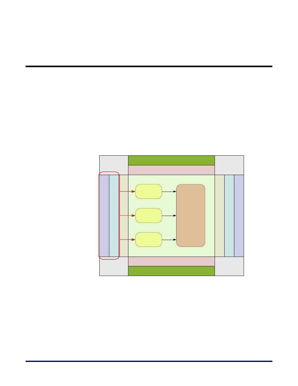
put the PHY into context. Figure 1 below shows a top-level view of a Speedster22iHD FPGA,
how the SerDes, IO and hard IP are organized, and how a memory interface would be built
using the hardened PHY and a soft controller.
Core Fabric
SerDes
SerDes
Protocol Hard IP
Protocol Hard IP
G
e
n
e
ra
l
P
u
rp
o
s
e
I
O
B
u
ff
e
r
IO
R
e
g
is
te
r
P
H
Y
a
n
d
D
L
L
H
a
rd
D
D
R
C
o
n
tr
o
lle
rs
G
e
n
e
ra
l
P
u
rp
o
s
e
I
O
B
u
ff
e
r
IO
R
e
g
is
te
r
P
H
Y
a
n
d
D
L
L
H
a
rd
D
D
R
C
o
n
tr
o
lle
rs
PLLs
PLLs
PLLs
PLLs
Soft DDR3
Controller
Application
Interface
QDRII+
Controller
RLDRAM3
Controller
Figure 1: Speedster22iHD Architecture for Memory Interface Design using Soft Controller
The IO in the Speedster22iHD devices is organized into 12 IO byte-lanes. Within this 12, there
are 10 DQ, 1 DQS and 1 DQSn IOs. The PHY implementation for all bits are the same, but
there are differences in top-level connectivity between the IOs implementing these different
functions. More importantly, there are differences in connectivity even for the same
DQS/DQSn bit across byte-lanes. This means that even for soft memory controller
implementations, there are IO placement restrictions, and it is important that Achronix
guidelines be followed to ensure that the particular memory interface PHY can be legally and
successfully implemented, and optimized to be able to timing close in the fabric.
