Byte lane building blocks, Ddr3 data byte lane – Achronix Speedster22i Memory PHY User Manual
Page 12

12
UG043, April 26, 2014
Byte Lane Building Blocks
As shown in Figure 5, the DDR PHY is made up of up to 9 data byte lanes (for a x72 mode
interface) and 4 CAC (Control, Address and Command) byte lanes, 1 one of them operating
at half rate, as denoted by the SD postfix. The building blocks inside these byte lanes are very
similar. This section will detail the building blocks in a data byte lane and then explain the
differences that can be seen in a CAC byte lane.
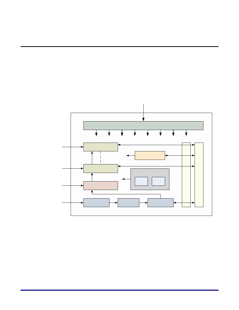
Figure 7 below provides a block level diagram of the building blocks inside a data byte lane.
Each of these blocks are described in more detail below.
ddr3_dq_bit
ddr3_dq_bit
x8
ddr3_dm_bit
ddr3_dq9_bit
postamble
ddr3_dqs_bit
Clk_mux
byte_lane_rxsy
write-leveling circuitry
b
y
te
_
la
n
e
_
s
d
_
lo
g
ic
DLL
(0.75T)
DLL
(0.25T)
b
y
te
_
la
n
e
_
lo
g
ic
DDR3 Data Byte Lane
Figure 7: DDR3 Data Byte Lane Building Blocks
Clk_mux: As the name implies, the clock mux takes in clocks coming in from the PLL, selects
and distributes them to the rest of the PHY logic.
ddr3_dq_bit: There are 8 of these dq data modules which feed the bidirectional buffers used
in data transmission and reception. The chapter on TX, RX and OE paths in Data Bits
provides a much closer look at the data paths through these dq data modules.
ddr3_dm_bit: This is the data mask bit controlling the masking operation at a byte level into
the PHY.
