Achronix Speedster22i Memory PHY User Manual
Page 13

UG043, April 26, 2014
13
ddr3_dq9_bit/postamble/ddr3_dqs_bit: These are the modules used to transmit and receive
dqs pulses to sample the data at dq. The chapter on DQS Clocking and Circuitry provides
more detail about the functionality of each of these blocks and how the dqs is adjusted to
ensure that the dq data is sampled optimally. The dqs output is provided to all of the dq and
dm bits as a clock. It can also be routed as an output to the FPGA fabric.
write leveling circuitry: There are 2 slave DLLs (sdlls), denoted as 0.25T and 0.75T to help
provide mechanisms to enable write leveling. These two DLLs take the reference clock as
input and produce shifted versions of this clock as inputs to the first stage of registering in
the dqs TX path.
byte_lane_rxsy: This module takes clocks and enables from the fabric as inputs and uses
them to time and generate the write and read pointers that are used when doing clock
domain transferring between the dqs clock domain and the core clock domain in the hard
FIFO on the data receive path.
byte_lane_logic/byte_lane_sd_logic: These modules provide control interfaces for muxing
signals between the hard DDR controller and a soft DDR controller (from the fabric).
A CAC byte lane is much simpler in its structure. There is a single bit module for every pad
that needs to be placed. A slave dll is used to provide for leveling capability and there is an
option to use a pad to have source synchronous clock be routed into the fabric. No additional
masking, pre/postambles or muxing is implemented or needed.
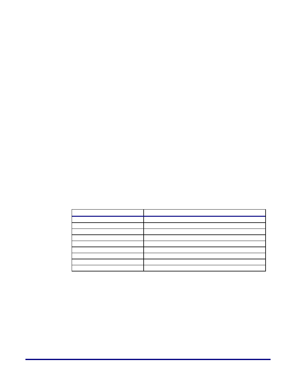
Table 4 below provides the mapping between the bits within each of these 4 CAC byte lanes
and the external DDR functions that they map to.
Table 4: CAC Byte Lane Mapping
DDR Function/Port
CAC Byte Lane Mapping
sd_cs_n[NUM_RANKS-1:0]
{cac_byte_0[1:0], cac_byte_1[1:0]}
sd_cke[NUM_RANKS-1:0]
{cac_byte_0[3:2], cac_byte_1[3:2]}
sd_odt[NUM_RANKS-1:0]
{cac_byte_0[5:4], cac_byte_1[5:4]}
sd_reset_n
{cac_byte_1[6]}
sd_a[15:0]
{cac_byte_1[9:8], cac_byte_2[3:0], cac_byte_sd[9:0]}
sd_ba[2:0]
{cac_byte_2[6:4]}
sd_we_n
{cac_byte_2[7]}
sd_cas_n
{cac_byte_2[8]}
sd_ras_n
{cac_byte_2[9]}
