Power-up and configuration sequence, Device power-up, Read non-volatile memories – Achronix Speedster22i Configuration User Manual
Page 5: Clear configuration memory
UG033, December 18, 2013
5
Power-Up and Configuration Sequence
The requirements for the power-up and configuration sequencing for Speedster22i HD
devices are illustrated in Table 1 and detailed below.
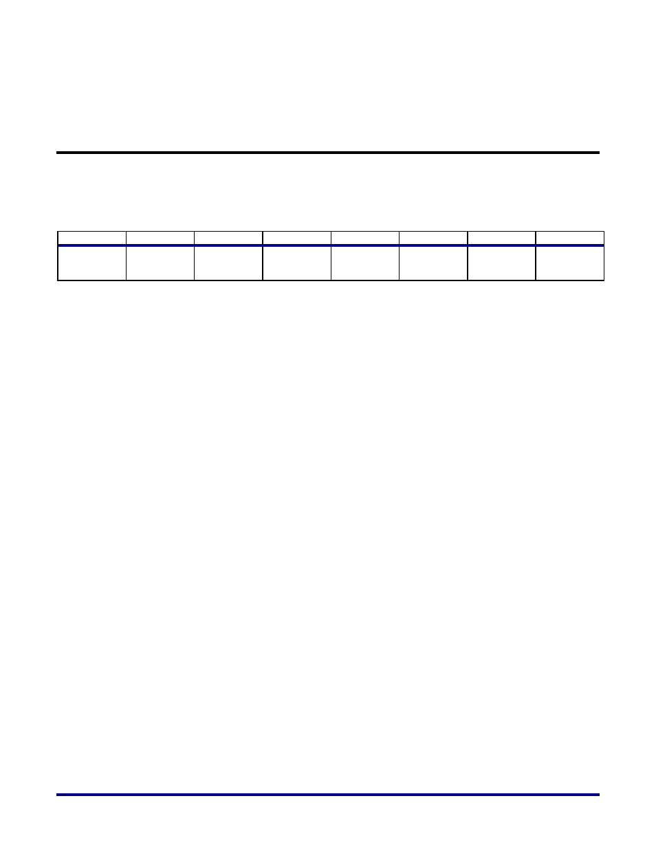
Table 1: Power-Up and Configuration Sequencing Steps
1
2
3
4
5
6
7
8
Device
power-up
Read non-
volatile
memories
Clear
configuration
memory
Bitstream
sync and
device ID
Load
configuration
bits
CRC check
Startup
sequence
User Mode
Device Power-Up
: The first step in bringing up the Speedster22i HD FPGAs is to
appropriately power it up. The Power Sequencing section of the Speedster22i Pin
Connections and Power Supply Sequencing User Guide provides an illustration of how the
power supplies and configuration related pins/signals need to be asserted to ensure a
successful FPGA power-up. To summarize these requirements:
a. Power-up all power supplies except for PA_VDD1, PA_VDD2 and VDDL to full rail.
b. Power-up PA_VDD1 and PA_VDD2 after VCC reaches full rail.
c. Bring CONFIG_RSTN low to assert the reset after PA_VDD1 and PA_VDD2 reach
full rail. This will perform an FPGA reset.
d. After some time (~ms), release CONFIG_RSTN. Once the FPGA is out of reset, steps
2 and 3 in Table 1 above, the reading of the non-volatile memories and the clearing of
the configuration memory, will be performed. After the configuration memory is
cleared, the CONFIG_STATUS signal will be released.
e. Power-up VDDL and wait for it to reach full rail. At this point, the FPGA is ready to
accept the bitstream.
Read Non-Volatile Memories
: After coming out of reset, the FCU reads the non-
volatile memory (fuse) contents and latches the data coming out. The fuses are factory set to
zero and can be programmed. Manufacturing and ID related fuses are set during ATE
testing. Fuses that pertain to design security are available for customers to program. Please
refer to the section on Design Security for operation details.
Clear Configuration Memory
: After the non-volatile memory is read, the FCU
enters the state to clear configuration memory. Configuration memory cells are 6-T SRAM
cells and are cleared one frame at a time by writing 0s into them. If this state is entered after a
full FPGA power-up, it is imperative that all configuration memory be cleared prior to