Overview – Achronix Speedster22i Configuration User Manual
Page 4
4
UG033, December 18, 2013
Overview
The configuration architecture in Speedster22i HD devices is composed of a few key pieces:
1. Configuration pins enabling data transfer from an external interface to the FPGA
2. FPGA Configuration Unit (FCU) which is the IP block containing the modes,
interfaces, state machines and other control logic to take data from the pins, perform
the necessary FPGA mode transitions and assemble the incoming data stream into a
form to be ultimately provided to the rest of the FPGA
3. Configuration registers in the IO ring and the configuration memory in the fabric
core which are the recipients of the bitstream data coming from the FCU
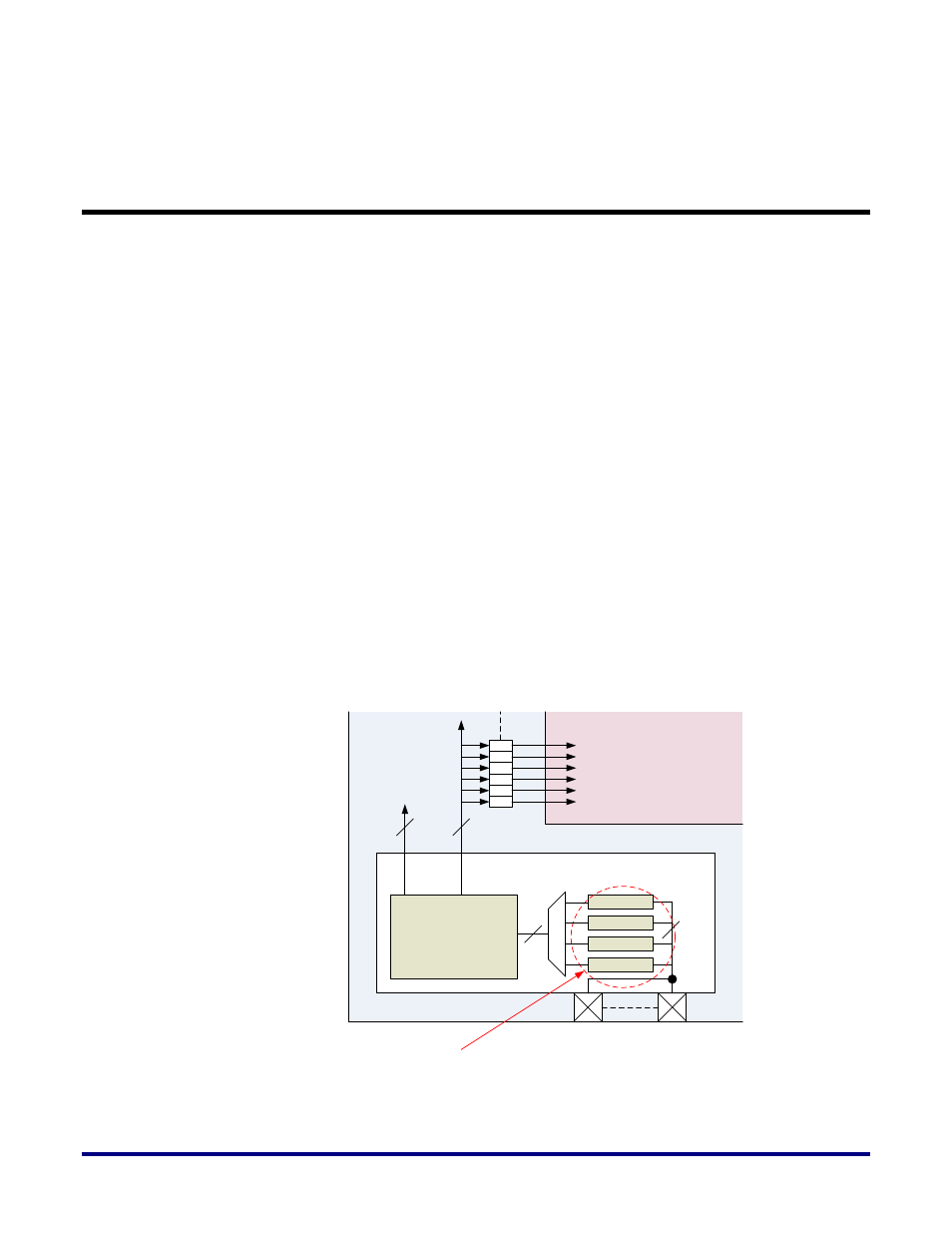
Figure 1 below provides a block level diagram showing the pieces of the configuration
architecture . Data from the configuration pins are brought into the FCU located in the IO
ring. Depending on the configuration mode, this data passes through one of four interfaces
and is then provided into the control logic and state machines in the FCU. At this point, the
data bus is standardized to a common interface. This data is interpreted here and then fans
out to the configuration registers in the IO ring and a bus to be parallelly loaded into column
based configuration memory frames in the FPGA fabric core. Once all of the configuration
bits have been successfully loaded, the FCU transitions the FPGA into user mode, providing
the capability for the user to provide stimuli and enable operation.
Core Fabric
IO Ring
Configuration Pins
Control Logic and
State Machines
JTAG
CPU
Flash x1
Flash x4
FPGA Configuration Unit (FCU)
Configuration Mode
Interfaces
To config bits
in IO ring
Parallel load of
config memory in
FPGA fabric core
Figure 1: FPGA Configuration Blocks