Achronix Speedster22i Configuration User Manual
Page 12
12
UG033, December 18, 2013
SPI Flash
Speedster22iHD FPGA
SCLK
HOLDN
DI
CSN
DO
SCK
HOLDN
SDI
CSN[0]
SDO[0]
SPI Flash
SCLK
HOLDN
DI
CSN
DO
SPI Flash
SCLK
HOLDN
DI
CSN
DO
SPI Flash
SCLK
HOLDN
DI
CSN
DO
CSN[1]
SDO[1]
CSN[2]
SDO[2]
CSN[3]
SDO[3]
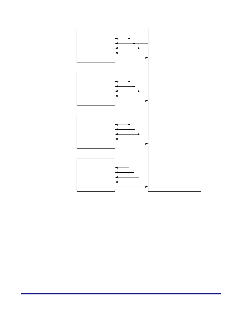
Figure 7: Flash Connectivity to Speedster22iHD FPGA in x4 Mode
When writing to the 4 Flash memories, the FPGA would pull the CSN for a single Flash
memory in turn, write the data and then move onto the next Flash memory by pulling the
corresponding CSN low. When reading from the 4 Flash memories, all CSN signals are
pulled low, and a x4 width configuration data is read from the Flash memories and
transferred to the FPGA through the SDO ports. Once bitstream operations are completed
(Flash memory contents are read), transitioning from the end of the bitstream to user mode is
done the same way as in CPU and Flash x1 modes.