Pin definitions – Cypress CY7C1443AV33 User Manual
Page 7
CY7C1441AV33
CY7C1443AV33,CY7C1447AV33
Document #: 38-05357 Rev. *G
Page 7 of 31
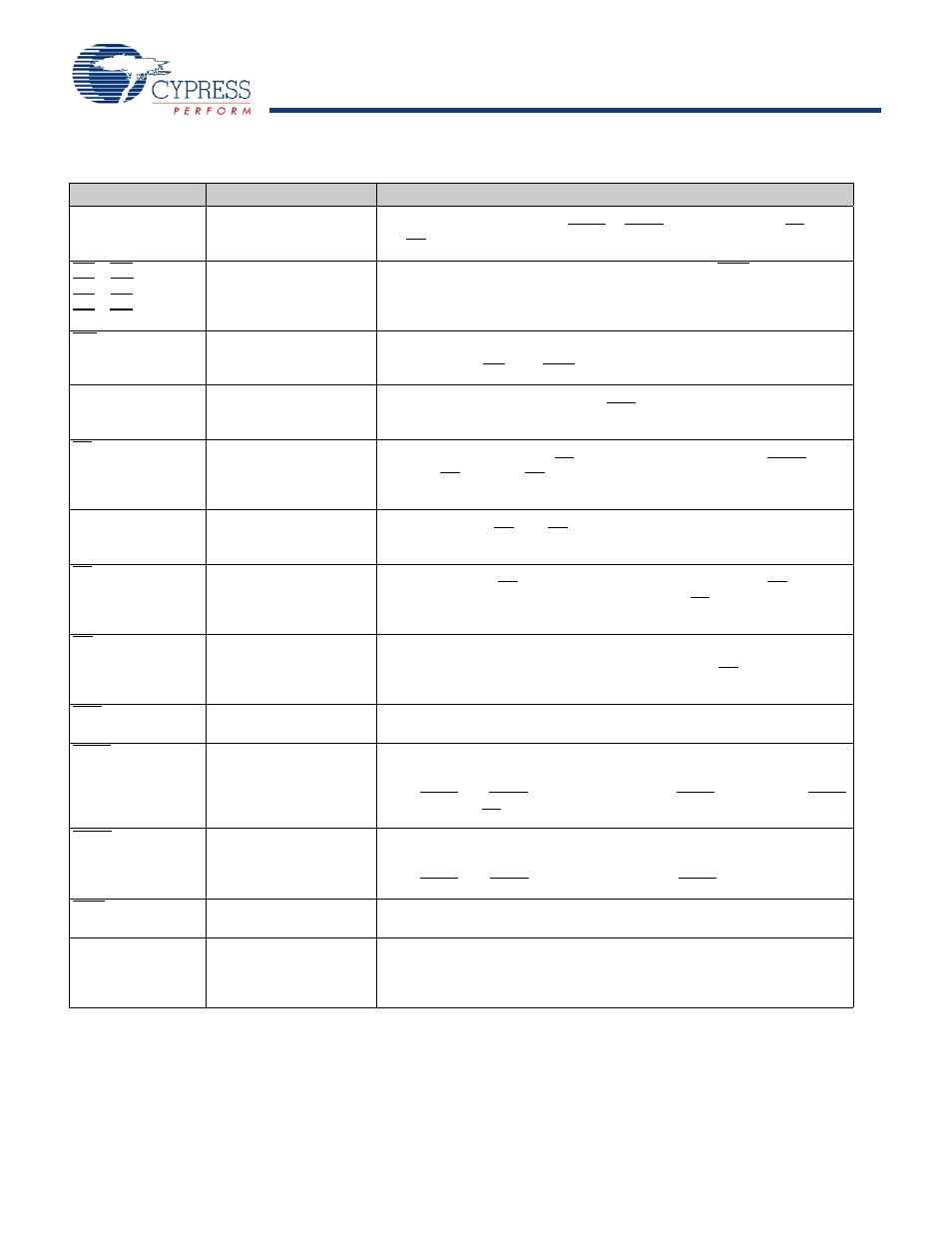
Pin Definitions
Name
IO
Description
A
0
, A
1
, A
Input-
Synchronous
Address Inputs Used to Select One of the Address Locations. Sampled
at the rising edge of the CLK if ADSP or ADSC is active LOW, and CE
1
,
CE
2
,
and
CE
3
are sampled active. A
[1:0]
feed the 2-bit counter.
BW
A
, BW
B
BW
C
, BW
D
,
BW
E
, BW
F
,
BW
G
, BW
H
Input-
Synchronous
Byte Write Select Inputs, Active LOW. Qualified with BWE to conduct byte
writes to the SRAM. Sampled on the rising edge of CLK.
GW
Input-
Synchronous
Global Write Enable Input, Active LOW. When asserted LOW on the rising
edge of CLK, a global write is conducted (ALL bytes are written, regardless
of the values on BW
X
and BWE).
CLK
Input-
Clock
Clock Input. Used to capture all synchronous inputs to the device. Also used
to increment the burst counter when ADV is asserted LOW, during a burst
operation.
CE
1
Input-
Synchronous
Chip Enable 1 Input, Active LOW. Sampled on the rising edge of CLK. Used
in conjunction with CE
2
and CE
3
to select/deselect the device. ADSP is
ignored if CE
1
is HIGH. CE
1
is sampled only when a new external address is
loaded.
CE
2
Input-
Synchronous
Chip Enable 2 Input, Active HIGH. Sampled on the rising edge of CLK. Used
in conjunction with CE
1
and CE
3
to select/deselect the device. CE
2
is sampled
only when a new external address is loaded.
CE
3
Input-
Synchronous
Chip Enable 3 Input, Active LOW. Sampled on the rising edge of CLK. Used
in conjunction with CE
1
and CE
2
to select/deselect the device. CE
3
is
assumed active throughout this document for BGA. CE
3
is sampled only when
a new external address is loaded.
OE
Input-
Asynchronous
Output Enable, Asynchronous Input, Active LOW. Controls the direction
of the IO pins. When LOW, the IO pins behave as outputs. When deasserted
HIGH, IO pins are tri-stated, and act as input data pins. OE is masked during
the first clock of a read cycle when emerging from a deselected state.
ADV
Input-
Synchronous
Advance Input Signal, Sampled on the Rising Edge of CLK. When
asserted, it automatically increments the address in a burst cycle.
ADSP
Input-
Synchronous
Address Strobe from Processor, Sampled on the Rising Edge of CLK,
Active LOW. When asserted LOW, addresses presented to the device are
captured in the address registers. A
[1:0]
are also loaded into the burst counter.
When ADSP and ADSC are both asserted, only ADSP is recognized. ASDP
is ignored when CE
1
is deasserted HIGH
ADSC
Input-
Synchronous
Address Strobe from Controller, Sampled on the Rising Edge of CLK,
Active LOW. When asserted LOW, addresses presented to the device are
captured in the address registers. A
[1:0]
are also loaded into the burst counter.
When ADSP and ADSC are both asserted, only ADSP is recognized.
BWE
Input-
Synchronous
Byte Write Enable Input, Active LOW. Sampled on the rising edge of CLK.
This signal must be asserted LOW to conduct a byte write.
ZZ
Input-
Asynchronous
ZZ “sleep” Input, Active HIGH. When asserted HIGH places the device in
a non-time-critical “sleep” condition with data integrity preserved. For normal
operation, this pin must be LOW or left floating. ZZ pin has an internal pull
down.