Partial truth table for read/write, Truth table for read/write, Function (cy7c1443av33)[2 – Cypress CY7C1443AV33 User Manual
Page 11: Function (cy7c1447av33)[2, 8
CY7C1441AV33
CY7C1443AV33,CY7C1447AV33
Document #: 38-05357 Rev. *G
Page 11 of 31
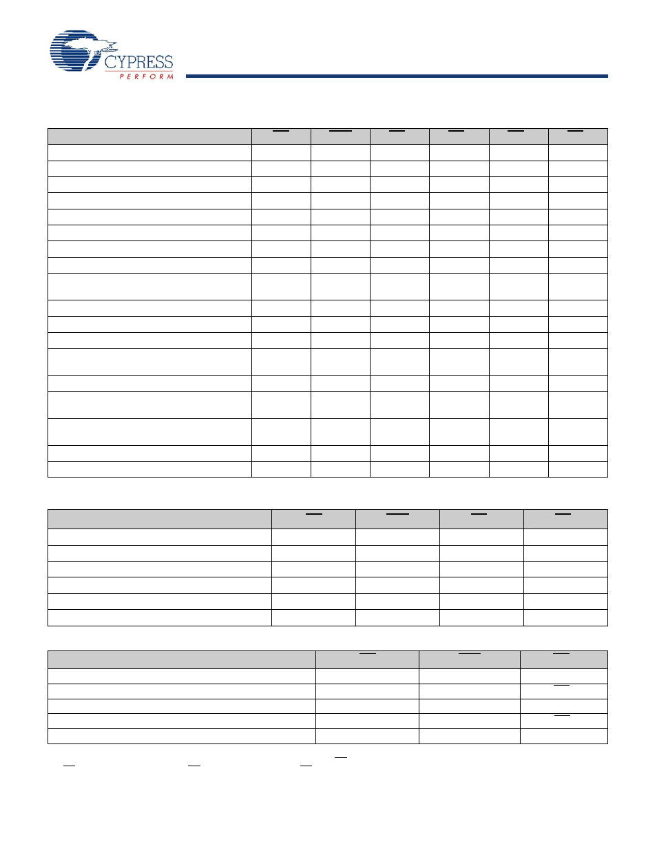
Partial Truth Table for Read/Write
Function (CY7C1441AV33)
GW
BWE
BW
D
BW
C
BW
B
BW
A
Read
H
H
X
X
X
X
Read
H
L
H
H
H
H
Write Byte A (DQ
A
, DQP
A
)
H
L
H
H
H
L
Write Byte B(DQ
B
, DQP
B
)
H
L
H
H
L
H
Write Bytes A, B (DQ
A
, DQ
B
, DQP
A
, DQP
B
)
H
L
H
H
L
L
Write Byte C (DQ
C
, DQP
C
)
H
L
H
L
H
H
Write Bytes C, A (DQ
C
, DQ
A,
DQP
C
, DQP
A
)
H
L
H
L
H
L
Write Bytes C, B (DQ
C
, DQ
B,
DQP
C
, DQP
B
)
H
L
H
L
L
H
Write Bytes C, B, A (DQ
C
, DQ
B
, DQ
A,
DQP
C
,
DQP
B
, DQP
A
)
H
L
H
L
L
L
Write Byte D (DQ
D
, DQP
D
)
H
L
L
H
H
H
Write Bytes D, A (DQ
D
, DQ
A,
DQP
D
, DQP
A
)
H
L
L
H
H
L
Write Bytes D, B (DQ
D
, DQ
A,
DQP
D
, DQP
A
)
H
L
L
H
L
H
Write Bytes D, B, A (DQ
D
, DQ
B
, DQ
A,
DQP
D
,
DQP
B
, DQP
A
)
H
L
L
H
L
L
Write Bytes D, B (DQ
D
, DQ
B,
DQP
D
, DQP
B
)
H
L
L
L
H
H
Write Bytes D, B, A (DQ
D
, DQ
C
, DQ
A,
DQP
D
,
DQP
C
, DQP
A
)
H
L
L
L
H
L
Write Bytes D, C, A (DQ
D
, DQ
B
, DQ
A,
DQP
D
,
DQP
B
, DQP
A
)
H
L
L
L
L
H
Write All Bytes
H
L
L
L
L
L
Write All Bytes
L
X
X
X
X
X
Truth Table for Read/Write
Function (CY7C1443AV33)
GW
BWE
BW
B
BW
A
Read
H
H
X
X
Read
H
L
H
H
Write Byte A - (DQ
A
and DQP
A
)
H
L
H
L
Write Byte B - (DQ
B
and DQP
B
)
H
L
L
H
Write All Bytes
H
L
L
L
Write All Bytes
L
X
X
X
Truth Table for Read/Write
Function (CY7C1447AV33)
GW
BWE
BW
X
Read
H
H
X
Read
H
L
All BW = H
Write Byte x – (DQ
x
and DQP
x
)
H
L
L
Write All Bytes
H
L
All BW = L
Write All Bytes
L
X
X
Notes
7. Table only lists a partial listing of the byte write combinations. Any Combination of BW
X
is valid Appropriate write is done based on which byte write is active.
8. BWx
represents any byte write signal BW
[A..H]
.To enable any byte write BW
x,
a Logic LOW signal should be applied at clock rise.Any number of bye writes can be
enabled at the same time for any given write.