Identification register definitions, Scan register sizes, Identification codes – Cypress CY7C1443AV33 User Manual
Page 17
CY7C1441AV33
CY7C1443AV33,CY7C1447AV33
Document #: 38-05357 Rev. *G
Page 17 of 31
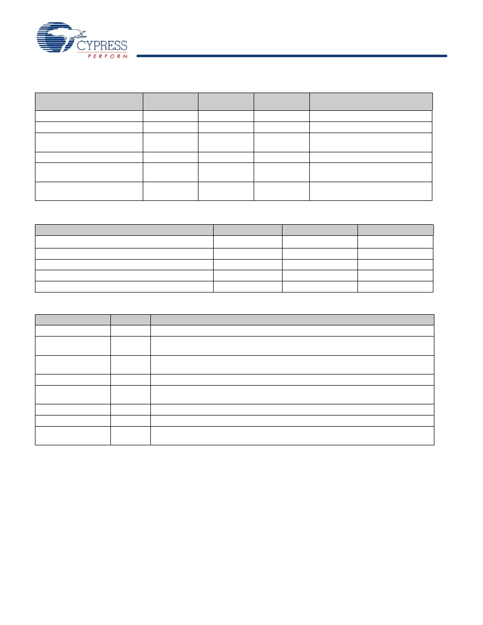
Identification Register Definitions
Instruction Field
CY7C1441AV33
(1M x 36)
CY7C1443AV33
(2M x 18)
CY7C1447AV33
(512K x 72)
Description
Revision Number (31:29)
000
000
000
Describes the version number.
Device Depth (28:24)
01011
01011
01011
Reserved for Internal Use
Architecture/Memory
Type(23:18)
000001
000001
000001
Defines memory type and architecture
Bus Width/Density(17:12)
100111
010111
110111
Defines width and density
Cypress JEDEC ID Code (11:1)
00000110100
00000110100
00000110100
Allows unique identification of SRAM
vendor.
ID Register Presence Indicator (0)
1
1
1
Indicates the presence of an ID
register.
Scan Register Sizes
Register Name
Bit Size (x36)
Bit Size (x18)
Bit Size (x18)
Instruction
3
3
3
Bypass
1
1
1
ID
32
32
32
Boundary Scan Order (165-ball FBGA package)
89
89
-
Boundary Scan Order (209-ball FBGA package)
-
-
138
Identification Codes
Instruction
Code
Description
EXTEST
000
Captures IO ring contents.
IDCODE
001
Loads the ID register with the vendor ID code and places the register between TDI and
TDO. This operation does not affect SRAM operations.
SAMPLE Z
010
Captures IO ring contents. Places the boundary scan register between TDI and TDO.
Forces all SRAM output drivers to a High-Z state.
RESERVED
011
Do Not Use: This instruction is reserved for future use.
SAMPLE/PRELOAD
100
Captures IO ring contents. Places the boundary scan register between TDI and TDO.
Does not affect SRAM operation.
RESERVED
101
Do Not Use: This instruction is reserved for future use.
RESERVED
110
Do Not Use: This instruction is reserved for future use.
BYPASS
111
Places the bypass register between TDI and TDO. This operation does not affect SRAM
operations.
Note
12. Bit #24 is “1” in the ID Register Definitions for both 2.5V and 3.3V versions of this device.