Timing diagrams, Continued) – Cypress CY7C1443AV33 User Manual
Page 23
CY7C1441AV33
CY7C1443AV33,CY7C1447AV33
Document #: 38-05357 Rev. *G
Page 23 of 31
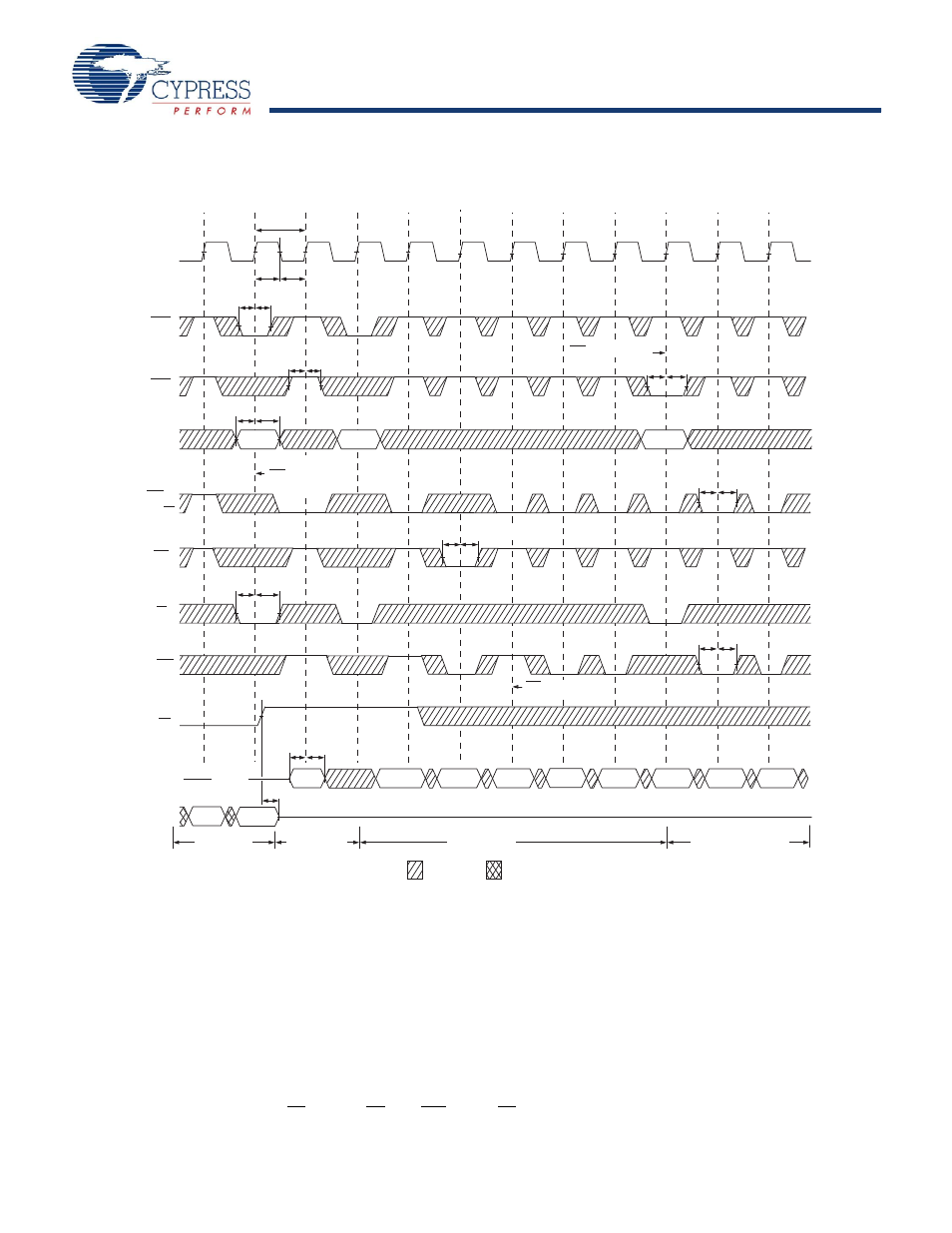
Figure 4. Write Cycle Timing
.
Timing Diagrams
(continued)
tCYC
t
CL
CLK
tADH
tADS
ADDRESS
t
CH
tAH
tAS
A1
tCEH
tCES
High-Z
BURST READ
BURST WRITE
D(A2)
D(A2 + 1)
D(A2 + 1)
D(A1)
D(A3)
D(A3 + 1)
D(A3 + 2)
D(A2 + 3)
A2
A3
Extended BURST WRITE
D(A2 + 2)
Single WRITE
tADH
tADS
tADH
tADS
t
OEHZ
tADVH
tADVS
tWEH
tWES
t
DH
t
DS
t
WEH
t
WES
Byte write signals are ignored for first cycle when
ADSP initiates burst
ADSC extends burst
ADV suspends burst
DON’T CARE
UNDEFINED
ADSP
ADSC
BWE,
BW
X
GW
CE
ADV
OE
Data in (D)
Data Out (Q)
Note
25. Full width write can be initiated by either GW LOW; or by GW HIGH, BWE LOW and BW
X
LOW
This manual is related to the following products: