I/o memory mapping – Rockwell Automation 1769-IT6 Compact I/O Thermocouple/mV Input Module User Manual
Page 17

Compact I/O Thermocouple/mV Input Module 17
Publication 1769-IN026C-EN-P - February 2010
I/O Memory Mapping
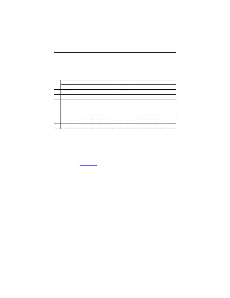
The input data file contains the analog values of the inputs.
The bits are defined as follows:
• Sx = General status bit for channels 0…5 and CJC sensors (S6 and S7). This bit is
set (1) when an error (over-range, under-range, open-circuit, or input data not valid)
exists for that channel. An ‘input data not valid’ condition is determined by the user
program. This condition occurs when the first analog-to-digital conversion is still in
progress, and after a new configuration has been sent to the module. Refer to
the Compact I/O Thermocouple/mV Input Module User Manual
69-UM004
, for additional details.
• OCx = Open-circuit detection bits indicate an open input circuit on channels 0…5
(OC0…OC5) and on CJC sensors CJC0 (OC6) and CJC1 (OC7). The bit is set (1)
when an open-circuit condition exists.
• Ux = Under-range flag bits for channels 0…5 and the CJC sensors (U6 and U7).
For thermocouple inputs, the under-range bit is set (1) when a temperature
measurement is below the normal operating range for a given thermocouple type.
For millivolt inputs, the under-range bit indicates a voltage that is below the normal
operating range. These bits can be used in the control program for error detection.
The bits are reset (0) by the module when within the normal operating range.
• Ox = Over-range flag bits for channels 0…5 and the CJC sensors (O6 and O7).
For thermocouple inputs, the over-range bit is set (1) when a temperature
measurement is above the normal operating range for a given thermocouple type.
For millivolt inputs, the over-range bit indicates a voltage that is above the normal
operating range. These bits can be used in the control program for error detection.
Input Data File
Wo
rd
Bit Position
15
14
13
12
11
10
9
8
7
6
5
4
3
2
1
0
0
Analog Input Data Channel 0
1
Analog Input Data Channel 1
2
Analog Input Data Channel 2
3
Analog Input Data Channel 3
4
Analog Input Data Channel 4
5
Analog Input Data Channel 5
6
OC7
OC6 OC5 OC4 OC3 OC2 OC1 OC0
S7
S6
S5
S4
S3
S2
S1
S0
7
U0
O0
U1
U0
U2
O2
U3
O3
U4
O4
U5
O5
U6
O6
U7
O7
