Calibration, Calibration registers, Calibration 2.5.1. calibration registers – Cirrus Logic CS5534-BS User Manual
Page 30: Offset register
CS5532/34-BS
30
DS755F3
2.5. Calibration
Calibration is used to set the zero and gain slope of
the ADC’s transfer function. The CS5532/34 offer
both self calibration and system calibration.
Note:
After the ADCs are reset, they are functional
and can perform measurements without
being calibrated (remember that the VRS bit
in the configuration register must be properly
configured). In this case, the converter will
utilize the initialized values of the on-chip
registers (Gain = 1.0, Offset = 0.0) to
calculate output words. Any initial offset and
gain errors in the internal circuitry of the chip
will remain.
2.5.1. Calibration Registers
The CS5532/34 converters have an individual off-
set and gain register for each channel input. The
gain and offset registers, which are used during
both self and system calibration, are used to set the
zero and gain slope of the converter’s transfer func-
tion. As shown in Offset Register section, one LSB
in the offset register is 1.835007966 X 2
-24
propor-
tion of the input span (bipolar span is 2 times the
unipolar span, gain register = 1.000...000 decimal).
The MSB in the offset register determines if the
offset to be trimmed is positive or negative (0 pos-
itive, 1 negative). Note that the magnitude of the
offset that is trimmed from the input is mapped
through the gain register. The converter can typi-
cally trim ±100 percent of the input span. As shown
in the Gain Register section, the gain register spans
from 0 to (64 - 2
-24
). The decimal equivalent mean-
ing of the gain register is
where the binary numbers have a value of either
zero or one (b
D29
is the binary value of bit D29).
While gain register settings of up to 64 - 2
-24
are
available, the gain register should never be set to
values above 40.
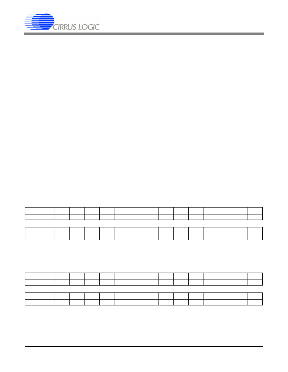
2.5.2. Gain Register
The gain register span is from 0 to (64-2
-24
). After Reset D24 is 1, all other bits are ‘0’.
2.5.3. Offset Register
One LSB represents 1.835007966 X 2
-24
proportion of the input span (bipolar span is 2 times unipolar span).
Offset and data word bits align by MSB. After reset, all bits are ‘0’.
The offset register is stored as a 32-bit, two’s complement number, where the last 8 bits are all 0.
D
b
D29
2
5
b
D28
2
4
b
D27
2
3
… b
D0
2
24
–
)
+
+
+
+
b
Di
2
24
–
i
+
(
)
i
0
=
29
∑
=
=
MSB
D30
D29
D28
D27
D26
D25
D24
D23
D22
D21
D20
D19
D18
D17
D16
NU
NU
2
5
2
4
2
3
2
2
2
1
2
0
2
-1
2
-2
2
-3
2
-4
2
-5
2
-6
2
-7
2
-8
0
0
0
0
0
0
0
1
0
0
0
0
0
0
0
0
D15
D14
D13
D12
D11
D10
D9
D8
D7
D6
D5
D4
D3
D2
D1
LSB
2
-9
2
-10
2
-11
2
-12
2
-13
2
-14
2
-15
2
-16
2
-17
2
-18
2
-19
2
-20
2
-21
2
22
2
-23
2
-24
0
0
0
0
0
0
0
0
0
0
0
0
0
0
0
0
MSB
D30
D29
D28
D27
D26
D25
D24
D23
D22
D21
D20
D19
D18
D17
D16
Sign
2
-2
2
-3
2
-4
2
-5
2
-6
2
-7
2
-8
2
-9
2
-10
2
-11
2
-12
2
-13
2
-14
2
-15
2
-16
0
0
0
0
0
0
0
0
0
0
0
0
0
0
0
0
D15
D14
D13
D12
D11
D10
D9
D8
D7
D6
D5
D4
D3
D2
D1
LSB
2
-17
2
-18
2
-19
2
-20
2
-21
2
-22
2
-23
2
-24
NU
NU
NU
NU
NU
NU
NU
NU
0
0
0
0
0
0
0
0
0
0
0
0
0
0
0
0