Offset and gain select, Filter rate select, Offset and gain select 2.3.8. filter rate select – Cirrus Logic CS5534-BS User Manual
Page 25
CS5532/34-BS
DS755F3
25
from VA+ and VA-. Their output voltage will be
limited to the VA+ voltage for a logic 1 and VA-
for a logic 0.
2.3.7. Offset and Gain Select
The Offset and Gain Select bit (OGS) is used to se-
lect the source of the calibration registers to use
when performing conversions and calibrations.
When the OGS bit is set to ‘0’, the offset and gain
registers corresponding to the desired physical
channel (CS1-CS0 in the selected Setup) will be ac-
cessed. When the OGS bit is set to ‘1’, the offset
and gain registers pointed to by the OG1-OG0 bits
in the selected Setup will be accessed. This feature
allows multiple calibration values (e.g. for different
gain settings) to be used on a single physical chan-
nel without having to re-calibrate or manipulate the
calibration registers.
2.3.8. Filter Rate Select
The Filter Rate Select bit (FRS) modifies the output
word rates of the converter to allow either 50 Hz or
60 Hz rejection when operating from a
4.9152 MHz crystal. If FRS is cleared to logic 0,
the word rates and corresponding filter characteris-
tics can be selected (using the Channel Setup Reg-
isters) from 7.5, 15, 30, 60, 120, 240, 480, 960,
1920, or 3840 Sps when using a 4.9152 MHz clock.
If FRS is set to logic 1, the word rates and corre-
sponding filter characteristics scale by a factor of
5/6, making the selectable word rates 6.25, 12.5,
25, 50, 100, 200, 400, 800, 1600, and 3200 Sps
when using a 4.9152 MHz clock. When using other
clock frequencies, these selectable word rates will
scale linearly with the clock frequency that is used.
VREF
C = 14pF
f =
2
φ Fine
1
V
≤ 8 mV
i = fV
C
os
os
n
φ Coarse
MCLK
16
VRS = 1; 1 V
≤ V
≤ 2.5 V
REF
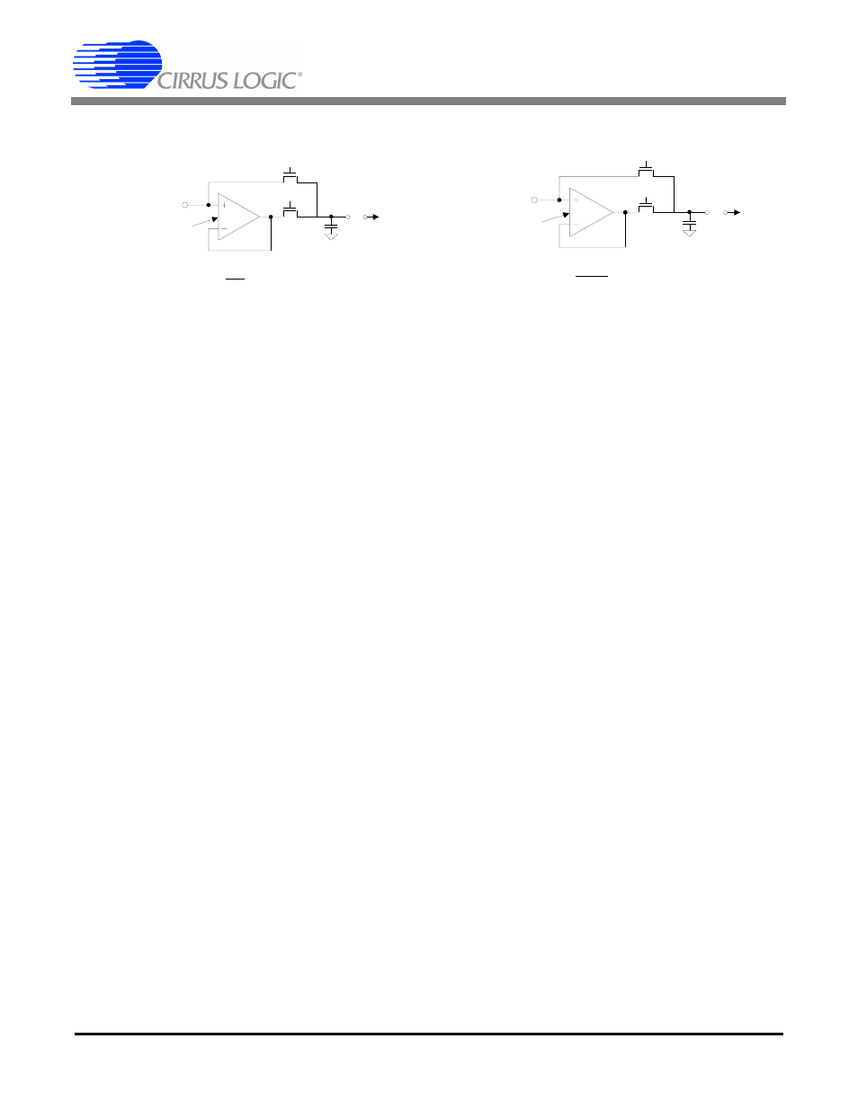
Figure 9. Input Reference Model when VRS = 1
VREF
C = 7 pF
f =
2
φ Fine
1
V
≤ 16 mV
i = fV
C
os
os
n
φ Coarse
MCLK
16
VRS = 0; 2.5 V < V
≤
VA+
REF
Figure 10. Input Reference Model when VRS = 0