Analog input span, Multiplexed settling limitations, Voltage noise density performance – Cirrus Logic CS5534-BS User Manual
Page 13
CS5532/34-BS
DS755F3
13
instrumentation amplifier is typically 1200 pA
over -40°C to +85°C (MCLK=4.9152 MHz).
The common-mode plus signal range of the instru-
mentation amplifier is (VA-) + 0.7 V to (VA+) -
1.7 V.
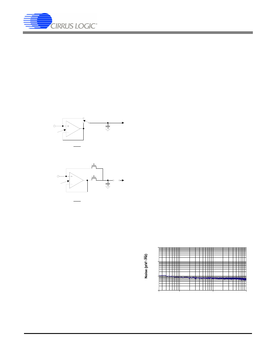
Figure 4
illustrates the input models for the ampli-
fiers. The dynamic input current for each of the
pins can be determined from the models shown.
Note:
The C=3.9pF and C = 14pF capacitors are
for input current modeling only. For physical
input capacitance see ‘Input Capacitance’
specification under Analog Characteristics.
2.1.1. Analog Input Span
The full-scale input signal that the converter can
digitize is a function of the gain setting and the ref-
erence voltage connected between the VREF+ and
VREF- pins. The full-scale input span of the con-
verter is ((VREF+) - (VREF-))/(GxA), where G is
the gain of the amplifier and A is 2 for VRS = 0, or
A is 1 for VRS = 1. VRS is the Voltage Reference
Select bit, and must be set according to the differen-
tial voltage applied to the VREF+ and VREF- pins
on the part. See section 2.3.5 for more details.
After reset, the unity gain buffer is engaged. With a
2.5 V reference this would make the full-scale input
range default to 2.5 V. By activating the instrumen-
tation amplifier (i.e. a gain setting other than 1) and
using a gain setting of 32, the full-scale input range
can quickly be set to 2.5/32 or about 78 mV. Note
that these input ranges assume the calibration regis-
ters are set to their default values (i.e. Gain = 1.0 and
Offset = 0.0).
2.1.2. Multiplexed Settling Limitations
The settling performance of the CS5532/34 in mul-
tiplexed applications is affected by the single-pole,
low-pass filter which follows the instrumentation
amplifier (see Figure 3). To achieve data sheet set-
tling and linearity specifications, it is recommend-
ed that a 22 nF C0G capacitor be used. Capacitors
as low as 10 nF or X7R type capacitors can also be
used with some minor increase in distortion for AC
signals.
2.1.3. Voltage Noise Density Performance
Figure 5 illustrates the measured voltage noise
density versus frequency from 0.025 Hz to 10 Hz
of a CS5532-BS. The device was powered with
±2.5 V supplies, using 30 Sps OWR, the 64x gain
range, bipolar mode, and with the input short bit
enabled.
AIN
Gain = 2, 4, 8, 16, 32, 64
C = 3 .9 pF
f =
Gain = 1
AIN
C = 14 pF
φ Coarse
1
φ Fine
1
V
≤ 12 mV
i = fV
C
os
os
n
V
≤ 8 mV
i = fV
C
os
os
n
MCLK
128
f =
MCLK
16
Figure 4. Input models for AIN+ and AIN- pins
1
10
100
1000
0.025
0.10
1.00
10.00
Frequency (Hz)
Figure 5. Measured Voltage Noise Density, 64x