1 analog pins, 1 voltage inputs, 2 current inputs – Cirrus Logic CS5484 User Manual
Page 7: 3 voltage reference, 4 crystal oscillator, 2 digital pins, 1 reset input, 2 cpu clock output, 3 digital outputs, Figure 1. oscillator connections
CS5484
DS981F3
7
2.1 Analog Pins
The CS5484 has two differential inputs (VIN1
VIN2)
for voltage input and two differential inputs
IIN1 IIN2)
for current1 and current2 inputs. The CS5484 also has
two voltage reference pins (VREF
) between which a
bypass capacitor should be placed.
2.1.1 Voltage Inputs
The output of the line voltage resistive divider or
transformer is connected to the VIN1
or VIN2 input
pins of the CS5484. The voltage channel is equipped
with a 10x, fixed-gain amplifier. The full-scale signal
level that can be applied to the voltage channel is
±250mV. If the input signal is a sine wave, the maximum
RMS voltage is 250mVp/
2
176.78mV
RMS
, which is
approximately 70.7% of maximum peak voltage.
2.1.2 Current Inputs
The output of the current-sensing shunt resistor,
transformer, or Rogowski coil is connected to the
IIN1
or IIN2 input pins of the CS5484. To
accommodate different current-sensing elements, the
current channel incorporates a programmable gain
amplifier (PGA) with two selectable input gains, as
described in the Config0 register description (see
section
6.6.1 Configuration 0 (Config0) – Page 0,
on page 35.) There is a 10x gain setting and
a 50x gain setting. The full-scale signal level for current
channels is ±50mV and ±250mV for 50x and 10x gain
settings, respectively. If the input signal is a sine wave,
the maximum RMS voltage is 35.35mV
RMS
or
176.78mV
RMS,
which is approximately 70.7% of
maximum peak voltage.
2.1.3 Voltage Reference
The CS5484 generates a stable voltage reference of
2.4V between the VREF
pins. The reference system
also requires a filter capacitor of at least 0.1µF between
the VREF
pins.
The reference system is capable of providing a
reference for the CS5484 but has limited ability to drive
external circuitry. It is strongly recommended that
nothing other than the required filter capacitor be
connected to the VREF
pins.
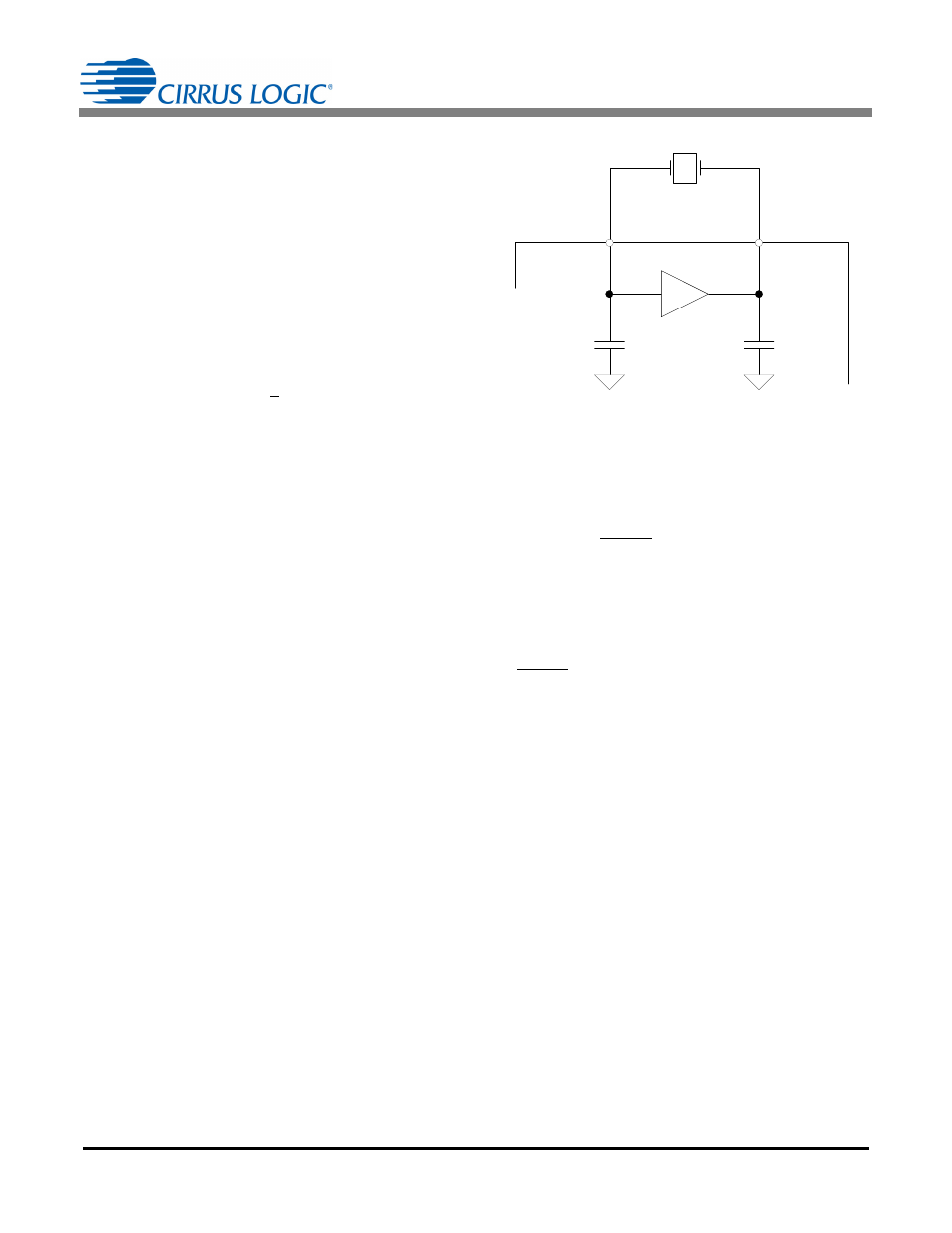
2.1.4 Crystal Oscillator
An external, 4.096MHz quartz crystal can be connected
to the XIN and XOUT pins, as shown in
. To re-
duce system cost, each pin is supplied with an on-chip
load capacitor.
Alternatively, an external clock source can be
connected to the XIN pin.
2.2 Digital Pins
2.2.1 Reset Input
The active-low RESET pin, when asserted for longer
than 120µs, will halt all CS5484 operations and reset
internal hardware registers and states. When
de-asserted, an initialization sequence begins, setting
default register values. To prevent erroneous
noise-induced resets to the CS5484, an external pull-up
resistor and a decoupling capacitor are necessary on
the RESET pin.
2.2.2 CPU Clock Output
A logic-level clock output (CPUCLK) is provided at the
crystal frequency to drive another CS5484 IC or
external microcontroller. Writing ‘1’ to bit CPUCLK_ON
of the Config0 register enables the CPU clock output.
After the CPU clock output is enabled, it can be disabled
only by a power-on reset (POR) or by writing ‘0’ to the
CPUCLK_ON bit. A hardware reset through pin/RESET
or a software reset instruction through the serial
interface will not disable the CPU clock output. Two
phase choices are available on the CPUCLK pin
through bit iCPUCLK of the Config0 register. Different
from the CPUCLK_ON bit, the iCPUCLK bit can be
cleared by a POR, a hardware reset, a software reset
instruction, or a register write.
2.2.3 Digital Outputs
The CS5484 provides four configurable digital outputs
(DO1-DO4). They can be configured to output energy
pulses, interrupt, zero-crossings, or energy directions.
Refer to section
6.6.2 Configuration 1 (Config1) – Page
on page 36 for more details.
XIN
XOUT
C1 = 22pF
C2 = 22pF
Figure 1. Oscillator Connections