Signal flow description, 1 analog-to-digital converters, 2 decimation filters – Cirrus Logic CS5484 User Manual
Page 17: 3 iir filters, 4 phase compensation, Cs5484
CS5484
DS981F3
17
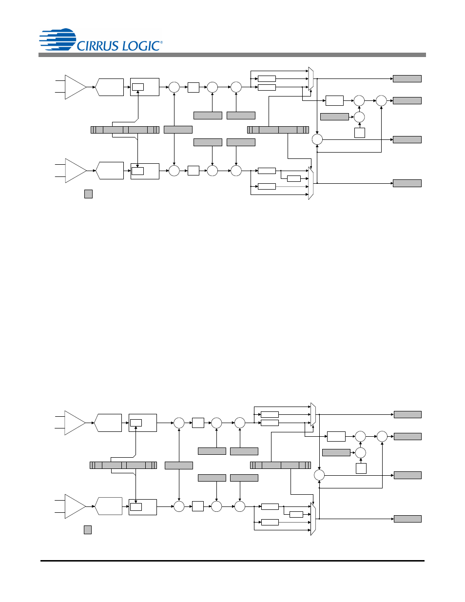
4. SIGNAL FLOW DESCRIPTION
The signal flow for voltage measurement, current
measurement, and the other calculations is shown in
,
, and
.
The signal flow consists of two current channels and two
voltage channels. The current and voltage channels
have differential input pins.
4.1 Analog-to-Digital Converters
All four input channels use fourth-order delta-sigma
modulators to convert the analog inputs to single-bit
digital data streams. The converters sample at a rate of
MCLK/8. This high sampling provides a wide dynamic
range and simplifies anti-alias filter design.
4.2 Decimation Filters
The single-bit modulator output data is widened to 24
bits and down sampled to MCLK/1024 with low-pass
decimation filters. These decimation filters are
third-order Sinc filters. The filter outputs pass through
an IIR "anti-sinc" filter.
4.3 IIR Filters
The IIR filters are used to compensate for the amplitude
roll-off of the decimation filters. The droop-correction
filter flattens the magnitude response of the channel out
to the Nyquist frequency, thus allowing for accurate
measurements of up to 2 kHz (MCLK = 4.096 MHz). By
default, the IIR filters are enabled. The IIR filters can be
bypassed by setting the IIR_OFF bit in the Config2
register.
4.4 Phase Compensation
Phase compensation changes the phase of voltage
relative to current by adding a delay in the decimation
filters. The amount of phase shift is set by the PC register
bits CPCCx[1:0] and FPCCx[8:0] for current channels.
Bits CPCCx[1:0] set the delay for the voltage channels.
MU
X
VIN1±
SINC
3
+
X
IIN1±
SINC
3
+
X
PGA
+
+
HPF
4
th
Order
ΔΣ
Modulator
4
th
Order
ΔΣ
Modulator
x10
X
DELAY
CTRL
X
X
X
2
MU
X
X
PMF
HPF
PMF
IIR
IIR
Phase
Shift
Config 2
X
Epsilon
DELAY
CTRL
INT
Registers
Q1
V1
P1
I1
SYS
GAIN
...
...
I1FLT[1:0]
V1FLT[1:0]
V1
DCOFF
I1
DCOFF
I1
GAIN
V1
GAIN
PC
...
...
FPCC1[8:0]
CPCC1[1:0]
...
Figure 9. Signal Flow for V1, I1, P1, and Q1 Measurements
MU
X
VIN2±
SINC
3
+
X
IIN2±
SINC
3
+
X
PGA
+
+
HPF
4
th
Order
ΔΣ
Modulator
4
th
Order
ΔΣ
Modulator
x10
X
DELAY
CTRL
X
X
X
2
MU
X
X
PMF
HPF
PMF
IIR
IIR
Phase
Shift
X
Epsilon
DELAY
CTRL
INT
Registers
Q2
V2
P2
I2
SYS
GAIN
V2
DCOFF
I2
DCOFF
I2
GAIN
V2
GAIN
PC
Config 2
...
...
I2FLT[1:0]
V2FLT[1:0]
...
...
FPCC2[8:0]
CPCC2[1:0]
...
Figure 10. Signal Flow for V2, I2, P2, and Q2 Measurements