6 register descriptions, Cs5484 – Cirrus Logic CS5484 User Manual
Page 35
CS5484
DS981F3
35
6.6 Register Descriptions
1.
“Default” = bit states after power-on or reset
2.
DO NOT write a “1” to any unpublished register bit or to a bit published as “0”.
3.
DO NOT write a “0” to any bit published as “1”.
4.
DO NOT write to any unpublished register address.
6.6.1 Configuration 0 (Config0)
–
Page 0, Address 0
Default = 0x40 0000
TSEL
Selects between Voltage Channel2 and Temperature.
0 = Selects Voltage Channel 2 (Default)
1 = Selects Temperature Sensor
[22]
Reserved.
iCPUCLK
CPU clock inversion control.
0 = CPU clock is same as MCLK (Default)
1 = Invert CPU clock to pin (CPU clock is inversion of MCLK)
CUCLK_ON
Enable CPUCLK to pad.
0 = Disable CPUCLK to pin (Default)
1 = Enable CPUCLK to pin
[19:15]
Reserved.
V2CAP[1:0]
Select the internal sampling capacitor size for V2 channel. Must be set to 00 for voltage
measurement.
00 = V2 used for voltage measurement (Default)
01 = V2 used for temperature measurement
10 = Reserved
11 = Reserved
[12:9]
Reserved.
INT_POL
Interrupt Polarity.
0 = Active low (Default)
1 = Active high
I2PGA[1:0]
Select PGA gain for I2 channel.
00 = 10x gain (Default)
10 = 50x gain
I1PGA[1:0]
Select PGA gain for I1 channel.
00 = 10x gain (Default)
10 = 50x gain
[3]
Reserved.
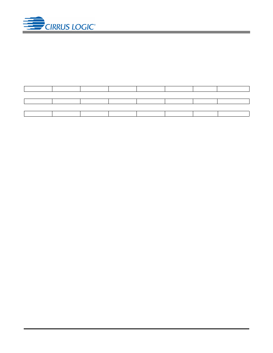
23
22
21
20
19
18
17
16
TSEL
1
iCPUCLK
CPUCLK_ON
-
-
-
-
15
14
13
12
11
10
9
8
-
V2CAP[1]
V2CAP[0]
0
0
-
-
INT_POL
7
6
5
4
3
2
1
0
I2PGA[1]
I2PGA[0]
I1PGA[1]
I1PGA[0]
-
NO_OSC
IZX_CH
VZX_CH