Pin descriptions, Digital pins and serial data i/o, Analog inputs / outputs – Cirrus Logic CS5484 User Manual
Page 6: Power supply connections, Clock generator, Thermal pad, Cs5484
CS5484
6
DS981F3
2. PIN DESCRIPTIONS
Digital Pins and Serial Data I/O
Digital Outputs
15,16,
17,18
DO1, DO2, DO3, DO4 — Configurable digital outputs for energy pulses, interrupt, energy
direction, and zero-crossings.
Reset
2
RESET — An active-low Schmitt-trigger input used to reset the chip.
Serial Data I/O
19,20
TX/SDO, RX/SDI — UART/SPI serial data output/input.
Serial Clock Input
21
SCLK — Serial clock for the SPI.
Chip Select
22
CS — Chip select for the UART/SPI.
Serial Mode Select
23
SSEL — Selects the type of serial interface, UART or SPI™. Logic level one - UART
selected. Logic level zero - SPI selected.
Operating Mode Select
24
MODE — Connect to VDDA for proper operation.
Analog Inputs/Outputs
Voltage Inputs
7,8,6,5
VIN1+, VIN1-, VIN2+, VIN2- — Differential analog inputs for the voltage channels.
Current Inputs
4,3,10,9
IIN1+, IIN1-, IIN2+, IIN2- — Differential analog inputs for the current channels.
Voltage Reference Input
12,11
VREF+, VREF- — The internal voltage reference. A 0.1µF bypass capacitor is required
between these two pins.
Power Supply Connections
Internal Digital Supply
27
VDDD — Decoupling pin for the internal 1.8V digital supply. A 0.1µF bypass capacitor is
required between this pin and GNDD.
Digital Ground
26
GNDD — Digital ground.
Positive Analog Supply
14
VDDA — The positive 3.3V analog supply.
Analog Ground
13
GNDA — Analog ground.
Clock Generator
Crystal In
Crystal Out
1,28
XIN, XOUT — Connect to an external quartz crystal. Alternatively, an external clock can be
supplied to the XIN pin to provide the system clock for the device.
CPU Clock Output
25
CPUCLK — Output of on-chip oscillator which can drive one standard CMOS load.
Thermal Pad
-
No Electrical Connection.
9
8
7
6
5
4
3
2
1
10
11
12
13
14
15
16
17
18
19
20
21
22
23
24
25
26
27
28
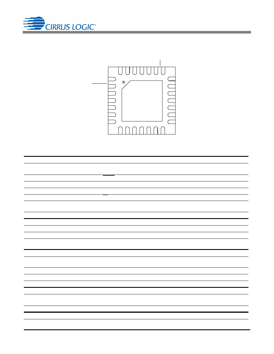
Top-Down View
28-pin QFN Package
Thermal Pad
XOUT
VDD
D
GNDD
CPU
C
LK
MODE
SSEL
CS
VI
N
1
-
II
N2-
II
N2+
VR
E
F
-
VREF+
GNDA
V
DDA
XIN
RESET
IIN1-
IIN1+
VIN2-
VIN2+
VIN1+
SCLK
RX/SDI
TX/SDO
DO4
DO3
DO2
DO1
Do Not Connect