2 spi read, Figure 19. control port timing, spi mode, 4 memory address pointer (map) – Cirrus Logic CS4349 User Manual
Page 27: 1 incr (auto map increment enable), 2 map (memory address pointer), Section 6.4.2, Figure 19, Cs4349
DS782F2
27
CS4349
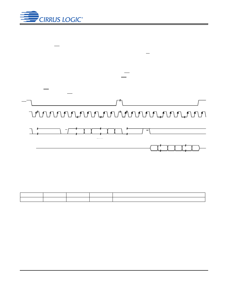
6.3.2
SPI Read
To read from the device, follow the procedure below while adhering to the values specified in
Characteristics - Control Port - SPI Format” on page 15
.
1. Bring CS low.
2. The address byte on the CDIN pin must then be 10011111 (R/W = 1).
3. CDOUT pin will then output the data from the register pointed to by the MAP, which is set during the
SPI write operation.
4. If the INCR bit (see
) is set to 1, keep CS low and continue providing clocks on CCLK to
read from multiple consecutive registers. Bring CS high when reading is complete.
5. If the INCR bit is set to 0 and further SPI reads from other registers are desired, it is necessary to bring
CS high, and follow the procedure detailed from step 1. If no further reads from other registers are
desired, bring CS high.
6.4
Memory Address Pointer (MAP)
6.4.1
INCR (Auto Map Increment Enable)
Default = ‘0’
0 - Disabled
1 - Enabled
6.4.2
MAP (Memory Address Pointer)
Default = ‘0000’
7
6
5
4
3
2
1
0
INCR
Reserved
Reserved
Reserved
MAP3
MAP2
MAP1
MAP0
0
0
0
0
0
0
0
0
M A P
MSB
LSB
DATA
b y te 1
b y te n
R/W
R/W
A D D R E S S
C H IP
ADDRESS
C H IP
MSB
LSB MSB
LSB
MAP = Memory Address Pointer, 8 bits, MSB first
High Impedance
1001111
1001111
CCLK
CDIN
CDOUT
CS
Figure 19. Control Port Timing, SPI Mode