8 analog output and filtering, Figure 17. passive single-ended output filter, 9 grounding and power supply arrangements – Cirrus Logic CS4349 User Manual
Page 23: 1 capacitor placement, Figure 17, Cs4349
DS782F2
23
CS4349
4.8
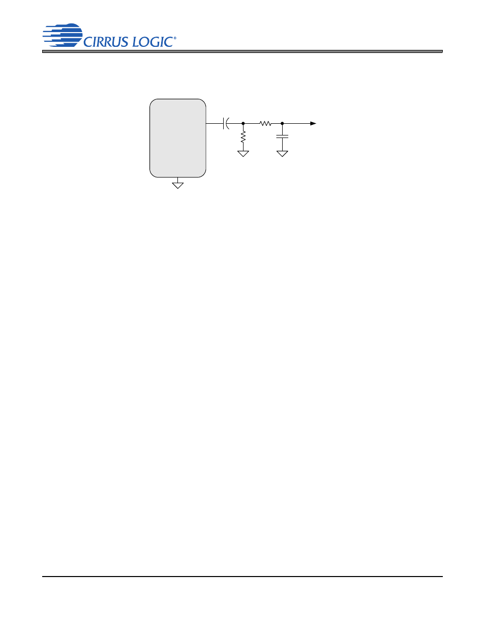
Analog Output and Filtering
The CS4349 requires a simple single-ended passive output design as shown in
4.9
Grounding and Power Supply Arrangements
As with any high-resolution converter, the CS4349 requires careful attention to power supply and grounding
arrangements if its potential performance is to be realized.
shows the recommended power
arrangements, with VA, VLC, and VLS connected to clean supplies. The use of split analog and digital
ground planes is not recommended. However, if planes are split between digital ground and analog ground,
the GND pins of the CS4349 should be connected to the analog ground plane.
All signals, especially clocks, should be kept away from the VBIAS, VFILT, and VQ pins in order to avoid
unwanted coupling into the DAC.
4.9.1
Capacitor Placement
Decoupling capacitors should be placed as close to the DAC as possible, with the low-value ceramic ca-
pacitor being the closest. To further minimize impedance, these capacitors should be located on the same
layer as the DAC. If desired, all supply pins may be connected to the same supply, but a decoupling ca-
pacitor should still be placed on each supply pin.
Note:
All decoupling capacitors should be referenced to GND.
The CDB4349 evaluation board demonstrates the optimum layout and power supply arrangements.
AOUTx +
3.3 µF
Analog
Output
2200 pF
+
10 k
GND
560
* See section 4.9 for ground connection details
Figure 17. Passive Single-Ended Output Filter
CS4349