Figure 1. output test load, Figure 2. maximum loading, Figure 3. thd+n vs output amplitude for va = 5.0 v – Cirrus Logic CS4349 User Manual
Page 11: Figure 4. thd+n vs output amplitude for va = 3.3 v, Figure 3, Figure 4, Figure 5, Figure 1, Figure 2, Cs4349
DS782F2
11
CS4349
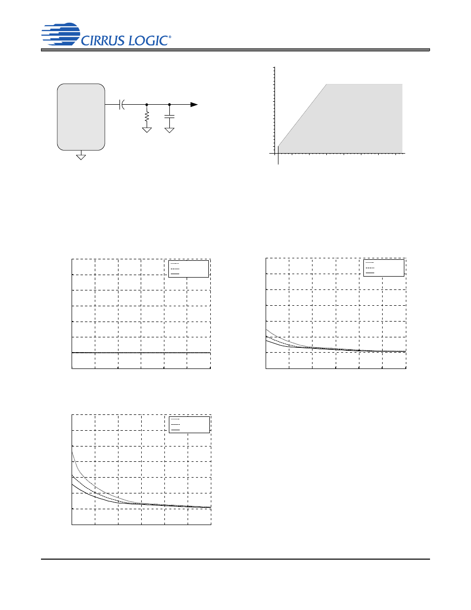
Figures 3 through 5 show typical THD+N performance for CS4349 devices that exhibit the maximum full
scale output voltages as specified in the DAC Analog Characteristics tables (see
and
decreasing VA, THD+N performance is increasingly affected by the full scale output voltage and
temperature, with higher full scale output voltage and lower temperatures corresponding to lower THD+N
performance.
AOUTx +
3.3 µF
Analog
Output
+
GND
R
L
C
L
100
50
75
25
2.5
5
10
15
Safe Operating
Region
Capacit
iv
e L
oad
--
C
(p
F
)
L
Resistive Load -- R (k
)
L
125
3
20
Figure 1. Output Test Load
Figure 2. Maximum Loading
CS4349
-3
-2.5
-2
-1.5
-1
-0.5
0
-100
-90
-80
-70
-60
-50
-40
-30
Output Amplitude(dB)
TH
D
+
N
(
d
B
)
TA = -40° C
TA = 25° C
TA = 85° C
-3
-2.5
-2
-1.5
-1
-0.5
0
-100
-90
-80
-70
-60
-50
-40
-30
Output Amplitude(dB)
THD
+
N (
d
B)
TA = -40° C
TA = 25° C
TA = 85° C
Figure 3. THD+N vs Output Amplitude for VA = 5.0 V
Figure 4. THD+N vs Output Amplitude for VA = 3.3 V
-3
-2.5
-2
-1.5
-1
-0.5
0
-100
-90
-80
-70
-60
-50
-40
-30
Output Amplitude(dB)
THD+
N (
d
B)
TA = -40° C
TA = 25° C
TA = 85° C
Figure 5. THD+N vs Output Amplitude for VA = 3.14 V