Figure 3. left justified up to 24-bit data, Figure 4. right justified data, 5 de-emphasis control – Cirrus Logic CS4341A User Manual
Page 9: Figure 5. de-emphasis curve, 6 recommended power-up sequence, Figure 3, Left justified up to 24-bit data, Figure 4, Right justified data, Figure 5
CS4341A
DS582F2
9
3.5
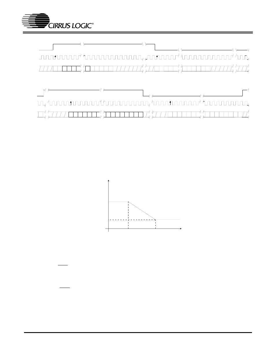
De-Emphasis Control
The device includes on-chip digital de-emphasis. The Mode Control 2 bits select either the 32, 44.1, or 48
kHz de-emphasis filter. Figure 5 shows the de-emphasis curve for F
s
equal to 44.1 kHz. The frequency
response of the de-emphasis curve will scale proportionally with changes in sample rate, Fs. Please see
section 5.2.3 for the desired de-emphasis control.
NOTE: De-emphasis is only available in Single-Speed Mode.
3.6
Recommended Power-up
Sequence
1. Hold RST low until the power supply is stable, and the master and left/right clocks are locked to
the appropriate frequences, as discussed in section 3.3. In this state, the control port is reset to its
default settings and VQ will remain low.
2. Bring RST high. The device will remain in a low power state with VQ low.
3. Load the desired register settings while keeping the PDN bit set to 1.
4. Set the PDN bit to 0. This will initiate the power-up sequence, which lasts approximately 50 µS
when the POR bit is set to 0. If the POR bit is set to 1, see section 3.7 for a complete description
of power-up timing.
L R C K
S C L K
L e ft C h a n n e l
R ig h t C h a n n e l
S D IN
+ 3 + 2 + 1
+ 5 + 4
M S B
-1 -2 -3 -4 -5
+ 3 + 2 + 1
+ 5 + 4
-1 -2 -3 -4
L S B
M S B
LS B
Figure 3. Left Justified up to 24-Bit Data
L R C K
S C L K
L e ft C h a n n e l
S D IN
-6 -5
-4 -3 -2 -1
-7
+ 1 + 2 + 3 + 4 +5
3 2 c lo c k s
M S B
R ig h t C h a n n e l
L S B
M S B
+ 1 + 2 + 3 +4 + 5
L S B
-6 -5
-4 -3 -2 -1
-7
M S B
Figure 4. Right Justified Data
Gain
dB
-10dB
0dB
Frequency
T2 = 15 µs
T1=50 µs
F1
F2
3.183 kHz
10.61 kHz
Figure 5. De-Emphasis Curve