Figure 7. control port timing, i2c mode, 3b i2c read, 3b i – Cirrus Logic CS4341A User Manual
Page 13: Figure 7, Control port timing, i2c mode, Cs4341a, C read
CS4341A
DS582F2
13
3.9.3b
I
2
C Read
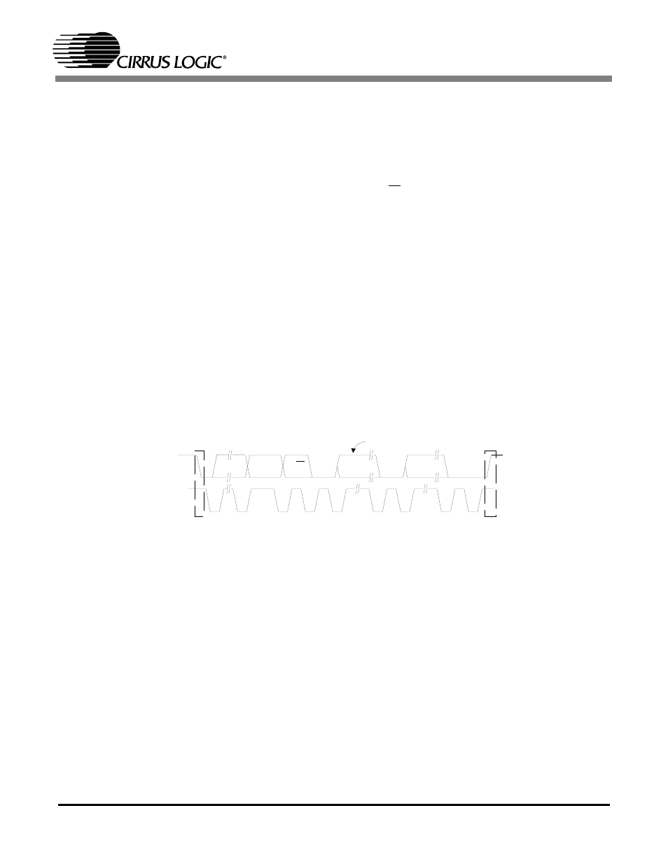
To read from the device, follow the procedure below while adhering to the control port
Switching Specifications.
1) Initiate a START condition to the I
2
C bus followed by the address byte. The upper 6 bits
must be 001000. The seventh bit must match the setting of the AD0 pin, and the eighth must
be 1. The eighth bit of the address byte is the R/W bit.
2) After transmitting an acknowledge (ACK), the device will then transmit the contents of
the register pointed to by the MAP. The MAP register will contain the address of the last
register written to the MAP, or the default address (see section 3.9.2) if an I
2
C read is the
first operation performed on the device.
3) Once the device has transmitted the contents of the register pointed to by the MAP, issue
an ACK.
4) If the INCR bit is set to 1, the device will continue to transmit the contents of successive
registers. Continue providing a clock and issue an ACK after each byte until all the desired
registers are read, then initiate a STOP condition to the bus.
5) If the INCR bit is set to 0 and further I
2
C reads from other registers are desired, it is nec-
essary to initiate a repeated START condition and follow the procedure detailed from step
1. If no further reads from other registers are desired, initiate a STOP condition to the bus.
S D A
S C L
0 01 0 00
A D 0
R /W
S ta rt
A C K
D AT A
1-8
A C K
D A TA
1-8
A C K
S top
N O T E
N O T E : If operation is a w rite, this byte contains the M em ory A ddress P ointer, M A P . If
operation is a read, this byte contains the data of the register pointed to by the M A P .
Figure 7. Control Port Timing, I
2
C Mode