3 system clocking, 4 digital interface format, Figure 2. i2s data – Cirrus Logic CS4341A User Manual
Page 8: 3 system clocking 3.4 digital interface format, Cs4341a
CS4341A
8
DS582F2
3.3
System Clocking
The device requires external generation of the master (MCLK), left/right (LRCK) and serial (SCLK)
clocks. The LRCK, defined also as the input sample rate (F
s
), must be synchronously derived from the
MCLK according to specified ratios. The specified ratios of MCLK to LRCK for each Speed Mode, along
with several standard audio sample rates and the required MCLK frequency, are illustrated in Tables 3-5.
* Requires MCLKDIV bit = 1 in the Mode Control 1 register (address 00h).
3.4
Digital Interface Format
The device will accept audio samples in several digital interface formats. The desired format is selected
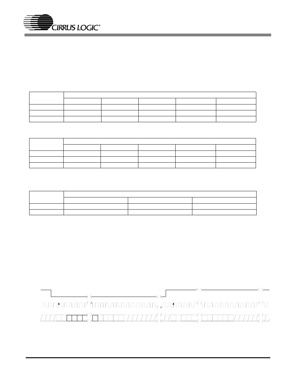
via the DIF0, DIF1 and DIF2 bits in the Mode Control 2 register (see section 5.2.2) . For an illustration of
the required relationship between LRCK, SCLK and SDIN, see Figures 2-4.
Sample Rate
(kHz)
MCLK (MHz)
256x
384x
512x
768x
1024x*
32
8.1920
12.2880
16.3840
24.5760
32.7680
44.1
11.2896
16.9344
22.5792
33.8688
45.1584
48
12.2880
18.4320
24.5760
36.8640
49.1520
Table 3. Single-Speed Mode Standard Frequencies
Sample Rate
(kHz)
MCLK (MHz)
128x
192x
256x
384x
512x*
64
8.1920
12.2880
16.3840
24.5760
32.7680
88.2
11.2896
16.9344
22.5792
33.8688
45.1584
96
12.2880
18.4320
24.5760
36.8640
49.1520
Table 4. Double-Speed Mode Standard Frequencies
Sample Rate
(kHz)
MCLK (MHz)
128x
192x
256x*
176.4
22.5792
33.8688
45.1584
192
24.5760
36.8640
49.1520
Table 5. Quad-Speed Mode Standard Frequencies
L R C K
S C L K
L e ft C h a n n e l
R ig h t C h a n n e l
S D IN
+3 +2 +1
+5 +4
M S B
-1 -2 -3 -4 -5
+3 +2 +1
+5 +4
-1 -2 -3 -4
M S B
LS B
LS B
Figure 2. I
2
S Data