Lvds interface (j7) – Ampro Corporation Single Board Computer 700 User Manual
Page 54
Chapter 3
Hardware
48
Reference Manual
ReadyBoard 700
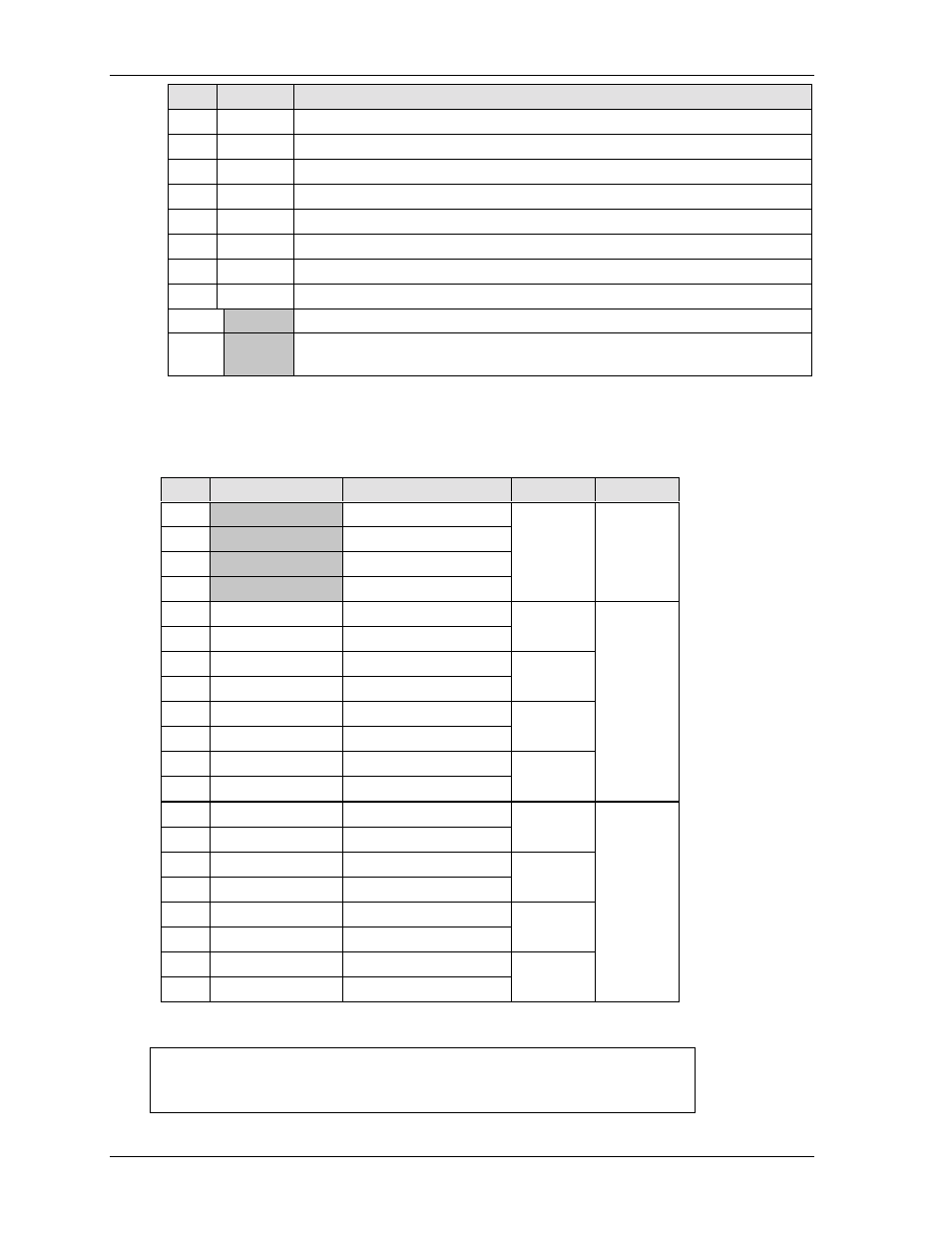
Pin #
Signal
Description
39
FPDEN
Flat Panel Data Enable – This signal to settle the horizontal display position.
40
FP0
Flat Panel Data Output 0 – Refer to pin-2 for more information.
41
FPCLKS
Flat Panel Shift clock – This signal can be inverted by jumper JP1.
42
VEEON
Voltage On – This signal is high (+5V) when ENVEE & Power Good are High
43
ENVDD
Flat Panel Enable VDD – This is power sequencing output for LCD driver
44
FPVS
Flat Panel VSync (FLM) – This signal is digital monitor equivalent of VSYNC
45
ENVEE
Flat Panel Enable VEE – This signal is used for power sequencing
46
FPHS
Flat Panel HSync (LP) – This signal is the digital monitor equivalent of HSYNC
47, 48
GND
Ground
49, 50
+12V
+12V (this voltage is supplied externally from the AT/ATX power supply input
connector. It may also be used by the PCI bus or ISA bus.
Notes: The shaded area denotes power or ground.
LVDS Interface (J7)
Table 3-22. LVDS Interface Pin/Signal Descriptions (J7)
Pin #
Signal
Description
Line
Channel
1
3.3V_Panel
+3.3V source
2
5V_Panel
+5V source
3
GND
Ground
4
GND
Ground
NA
NA
5
LVDS_Y0M
Data Negative Output
6
LVDS_Y0P
Data Positive Output
0
7
LVDS_Y1M
Data Negative Output
8
LVDS_Y1P
Data Positive Output
1
9
LVDS_Y2M
Data Negative Output
10
LVDS_Y2P
Data Positive Output
2
11
LVDS_CLKYM
Clock Negative Output
12
LVDS_CLKYP
Clock Positive Output
Clock
Channel 1
13
LVDS_Z0M
Data Negative Output
14
LVDS_Z0P
Data Positive Output
0
15
LVDS_Z1M
Data Negative Output
16
LVDS_Z1P
Data Positive Output
1
17
LVDS_Z2M
Data Negative Output
18
LVDS_Z2P
Data Positive Output
2
19
LVDS_CLKZM
Clock Negative Output
20
LVDS_CLKZP
Clock Positive Output
Clock
Channel 2
Notes: The shaded area denotes power or ground.
NOTE
Pins 5-12 constitute 1
st
channel interface of two channels, or a
single channel interface. Pins 13-20 constitute 2
nd
channel
interface of a two channel interface.