Ampro Corporation Single Board Computer 700 User Manual
Page 42
Chapter 3
Hardware
36
Reference Manual
ReadyBoard 700
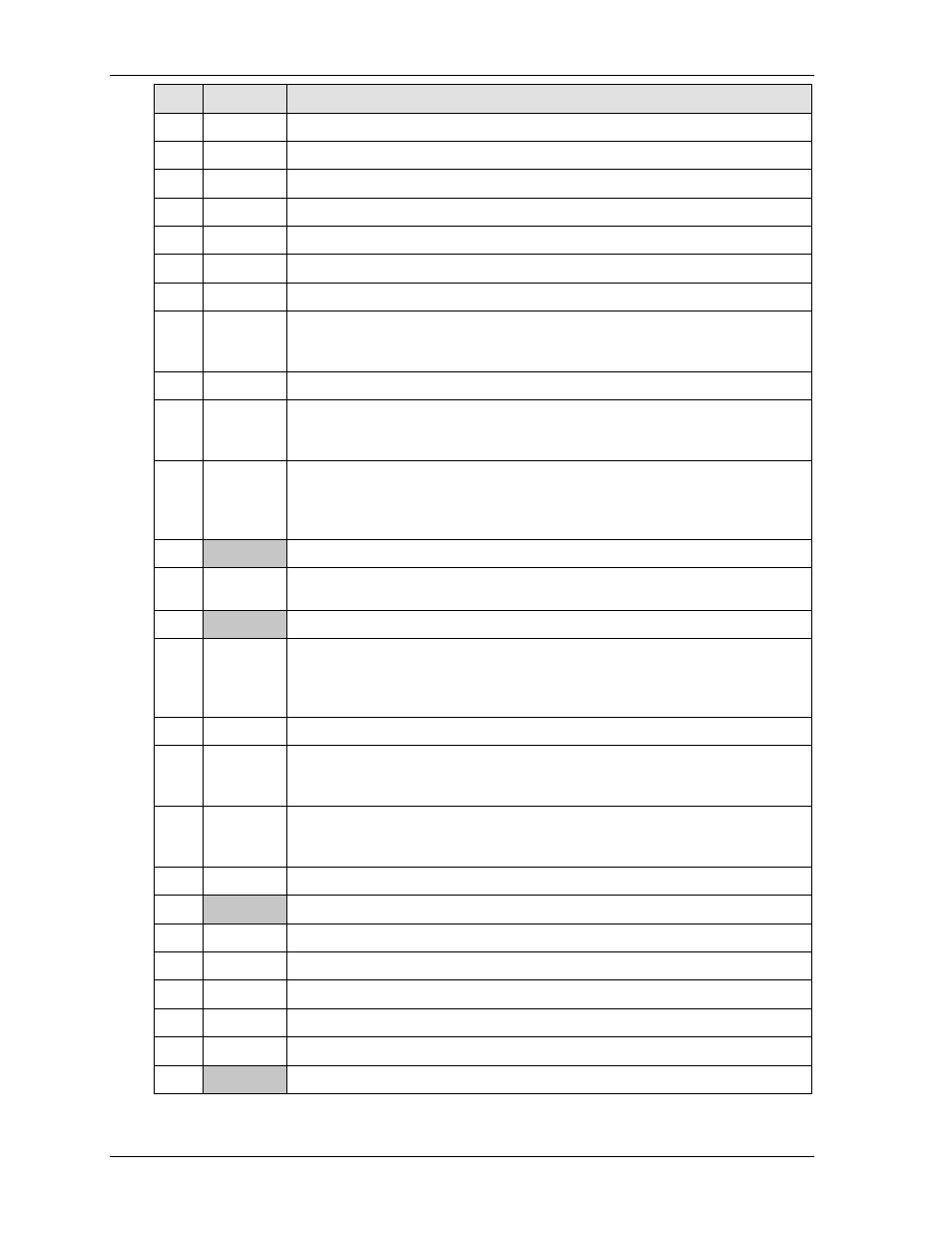
Pin #
Signal
Description
25
CFD2
Connected through 4.7k ohm resister to ground
26
CFD1
Connected through 4.7k ohm resister to ground
27
SDD11
Secondary Disk Data 11 – Refer to SDD3 on pin-2 for more information.
28
SDD12
Secondary Disk Data 12 – Refer to SDD3 on pin-2 for more information.
29
SDD13
Secondary Disk Data 13 – Refer to SDD3 on pin-2 for more information.
30
SDD14
Secondary Disk Data 14 – Refer to SDD3 on pin-2 for more information.
31
SDD15
Secondary Disk Data 15 – Refer to SDD3 on pin-2 for more information.
32
SDCS3*
Secondary Slave/Master Chip Select – This signal, along with CE1*, is used to
select the CompactFlash card and indicate to the card when a byte or word
operation is being performed. This signal always accesses the odd byte of word.
33
NC
Not Connected (VS1*)
34
SDIOR*
Secondary Device I/O Read/Write Strobe – This signal is generated by the host
and gates the I/O data onto the bus from the CompactFlash card when the card is
configured to use the I/O interface.
35
SDIOW*
Secondary Device I/O Read/Write Strobe – This signal is generated by the host
and clocks the I/O data on the Card Data bus into the CompactFlash card
controller registers when the card is configured to use the I/O interface. The clock
occurs on the negative to positive edge of the signal (trailing edge).
36
VCC
+5 volts +/-5%
37
IRQ15
Interrupt Request 15 – IRQ 15 is asserted by drive (CF) when it has a pending
interrupt (PIO transfer of data to or from the drive to the host).
38
VCC
+5 volts +/-5%
39
MASTER* Master/Slave – This signal is determined by jumper JP4 and is used to configure
this device as a Master or a Slave. When this pin is grounded (jumper inserted),
this device is configured as Master. When this pin is open (jumper removed), this
device is configured as Slave (Default).
40
NC
Not Connected (VS2*)
41
RSTIDE*
Secondary IDE Reset – This input signal is the active low hardware reset from the
host. If this pin goes high, it is used as the reset signal. This pin is driven high at
power-up, causing a reset, and if left high will cause another reset.
42
SDIORDY
Secondary Device I/O-DMA Channel Ready – When negated, extends the host
transfer cycle of any host register access when the drive is not ready to respond to
a data transfer request. High impedance if asserted.
43
NC
Not Connected (InpAck)
44
VCC
+5 volts +/-5%
45
IDE LED2
IDE Activity – Indicates CF activity to yellow IDE LED (D4) oncard edge.
46
SD33-66
SD33/66 Sense –Senses which DMA mode to use for the CompactFlash card.
47
SDD8
Secondary Disk Data 8 – Refer to SDD3 on pin-2 for more information.
48
SDD9
Secondary Disk Data 9 – Refer to SDD3 on pin-2 for more information.
49
SDD10
Secondary Disk Data 10 – Refer to SDD3 on pin-2 for more information.
50
GND
Digital Ground
Notes: The shaded area denotes power or ground. The signals marked with * = Negative true logic.