Communication Concepts AN758 User Manual
Page 7
AR
C
HIVE INF
O
RMA
TI
O
N
PRODUCT TRANSFERRED T
O
M/A
–
COM
AN758
7
RF Application Reports
The input transformer is equal to what is used with the
power amplifier, but has a 4:1 impedance ratio. The required
minimum inductance in the one turn secondary (Figures 3
and 4) being considerably higher in this case,
2
πf
4R
=
12.5
4 x 12.5
= 4.0
µH
the A
L
product of the core is barely sufficient. The measured
inductances between a number of cores range 3.8 – 4.1
µH.
This formula also applies to the output transformer, which
is a 1:1 balun. The required minimum inductance at 2 MHz
is 16
µH, amounting to 11 turns on a Ferroxcube
2616P-A100–4C4 pot core, which was preferred over a
toroid because of ease of mounting and other physical
features. Although twisted wire line would be good at this
power level, the transformer was wound with RG-196 coaxial
cable, which is also used later for module-driver
interconnections.
The required worst case driver output is s 4 x 12 W =
48 W. The optimum P
out
with the 1:1 output transformer is:
50
V
RMS
x V
RMS
=
50
67.7
x 67.7 = 92 W.
The MRF 427 is specified for a 25 W power output. Having a
good h
FE
versus I
C
linearity, the 1 to 2 load mismatch has an
effect of 2 – 3 dB in the IMD at the 10 power level, and the
reduced efficiency in the driver is insignificant regarding the
total supply current in the system.
The component values for the base input network and
the feedback were established with the aid of a computer,
and information on the device data sheet, as described
earlier with the 300 W module. The HF compensation was
done in a similar manner as well. Neither amplifier employs
LF compensation. C7 and C8 are dc blocking capacitors,
and their value is not critical.
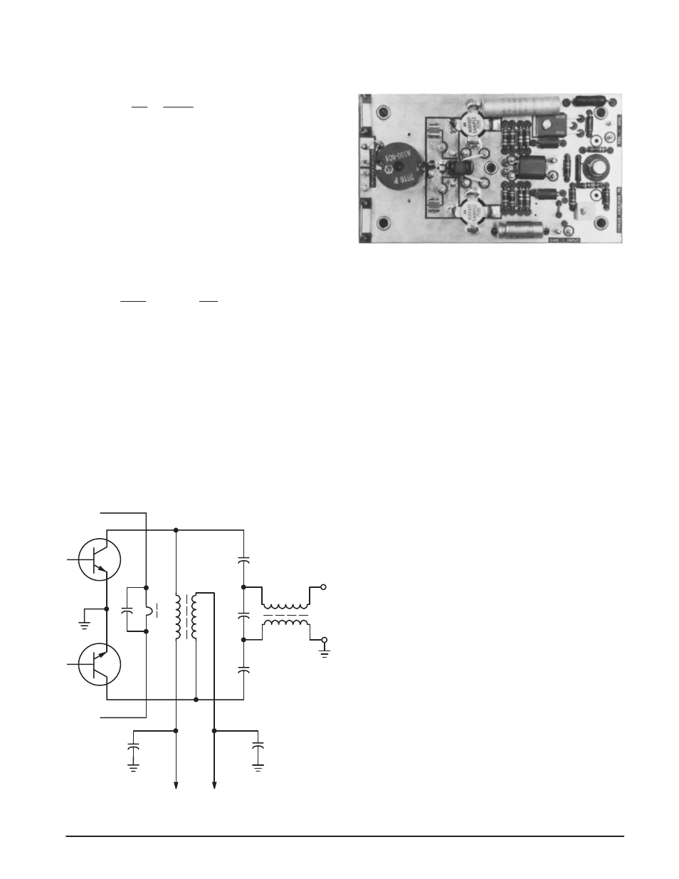
In T2 (Figure 7), b and c represent the RF center tap,
but are separated in both designs — partly because of circuit
lay-out convenience and partly for stabilization purposes.
L5
C5
a
c
b
d
C9
C10
C8
C6
C7
T2
T3
Figure 7.
The test data of the driver is presented later along with
the final test results.
Figure 8. Driver Amplifier Board Layout
COMBINING FOUR 300 W POWER MODULES
The Input Power Divider
The purpose of the power divider is to divide the input
power into four equal sources, providing an amount of
isolation between each. The outputs are designed for 50
Ω
impedance, which sets the common input at 12.5
Ω. This
requires an additional 4:1 step down transformer to provide
a 50
Ω load for the driver amplifier. Another requirement is
a 0
° phase shift between the input and the 50 Ω outputs,
which can be accomplished with 1:1 balun transformers. (a,
b, c and d in Figure 10.) For improved low frequency isolation
characteristics the line impedance must be increased for the
parallel currents. This can be done, without affecting the
physical length of the line, by loading the line with magnetic
material. In this type transformer, the currents cancel, making
it possible to employ high permeability ferrite and a relatively
short physical length for the transmission lines. In an
absolutely balanced condition, no power will be dissipated
in the magnetic cores, and the line losses are reduced. The
minimum required inductance for each line can be calculated
as shown for the driver amplifier output transformer, which
gives a number of 16
µH minimum at 2 MHz. A low
inductance value degrades the isolation characteristics
between the 50
Ω output ports, to maintain a low VSWR in
case of a change in the input impedance of one or more
of the power modules. However, because of the base
compensation networks, the power splitter will never be
subjected to a completely open or shorted load.
The purpose of the balancing resistors (R) is to dissipate
any excess power, if the VSWR increases. Their optimum
values, which are equal, are determined by the number of
50
Ω sources assumed unbalanced at one time, and the
resistor values are calculated accordingly.
Examining the currents with one load open, it can be seen
that the excess power is dissipated in one resistor in series
with three parallel resistors. Their total value is 50 – 12.5
= 37.5
Ω. Similarly, if two loads are open, the current flows
through one resistor in series with two parallel resistors,
totaling 37.5
Ω again. This situation is illustrated in Figure 11.