Communication Concepts AN758 User Manual
Page 6
AR
C
HIVE INF
O
RMA
TI
O
N
PRODUCT TRANSFERRED T
O
M/A
–
COM
AN758
6
RF Application Reports
The 1:4 output transformer is not the optimum in this case,
but it is the closest practical at these power levels. The
optimum power output at 50 V supply voltage and 50
Ω load
is:
V
RMS
= 4 x (V
CC
– V
CE(sat)
x 0.707) = 135.75 V,
when V
CE(sat)
= 2 V
50
135.75
= 2.715 A, P
out
= 2.715 x 135.75 = 368.5 W
I =
The optimum V
CC
at P
out
= 300 W would be:
V
CC
= V
CE(sat)
+ ( R
in
x 2 P
out
) =
2 + ( 6.25 x 300)
= 45.3 V
The above indicates that the amplifier sees a lower load
line, and the collector efficiency will be lowered by 1 – 2%.
The linearity at high power levels is not affected, if the device
h
FE
is maintained at the increased collector currents. The
linearity at low power levels may be slightly decreased due
to the larger mismatch of the output circuit.
The required characteristic line impedance (a and b,
Figure 3) for a 1:4 impedance transformer is:
√R
in
R
L
=
√12.5 x 50 = 25 Ω, enables the use of standard miniature
25
Ω coaxial cable (i.e., Microdot 260-4118-000) for the
transmission lines. The losses in this particular cable at
30 MHz are 0.03 dB/ft. With a total line length of 2 x 16.8
″
(2 x 4 x 4.2
″), the loss becomes 0.084 dB, or
10 antilog 0.084 dB
300
= 5.74 W.
300 –
Ǔ
ǒ
For the ferrite material employed, Stackpole grade #11 (or
equivalent Indiana General Q1) the manufacturers data is in-
sufficient for accurate core loss calculations
(6)
The B
H
curves
indicate that 100 – 150 gauss is well in the linear region.
The toroids measure 0.87
″ x 0.54″ x 0.25″, and the 16.8″
line length figured above, totals to 16 turns if tightly wound,
or 12 – 14 turns if loosely wound. The flux density can then
be calculated as:
2
πfnA
V
max
x 102
B
max
=
where:
f = Frequency in MHz
n = Total number of turns.
A = Cross sectional area of the toroid in cm
2
.
V = Peak voltage across the 50
Ω load,
= 173 V
50
300
Ǔ
ǒ
0.707
50
Ǔ
ǒ
6.28 x 2 x 28 x .25
86.5 x 10
2
B
max
(for each toroid) =
= 98.3 gauss
Practical measurements showed the core losses to be
negligible compared to the line losses at 2 MHz and 30 MHz.
However, the losses increase as the square of B
max
at low
frequencies.
With the amount of HF compensation dependent upon
circuit layout and the exact transformer construction, no
calculations were made on this aspect for the input (or
output) transformers. C3, C4, and C6 were selected by
employing adjustable capacitors on a prototype whose
values were then measured.
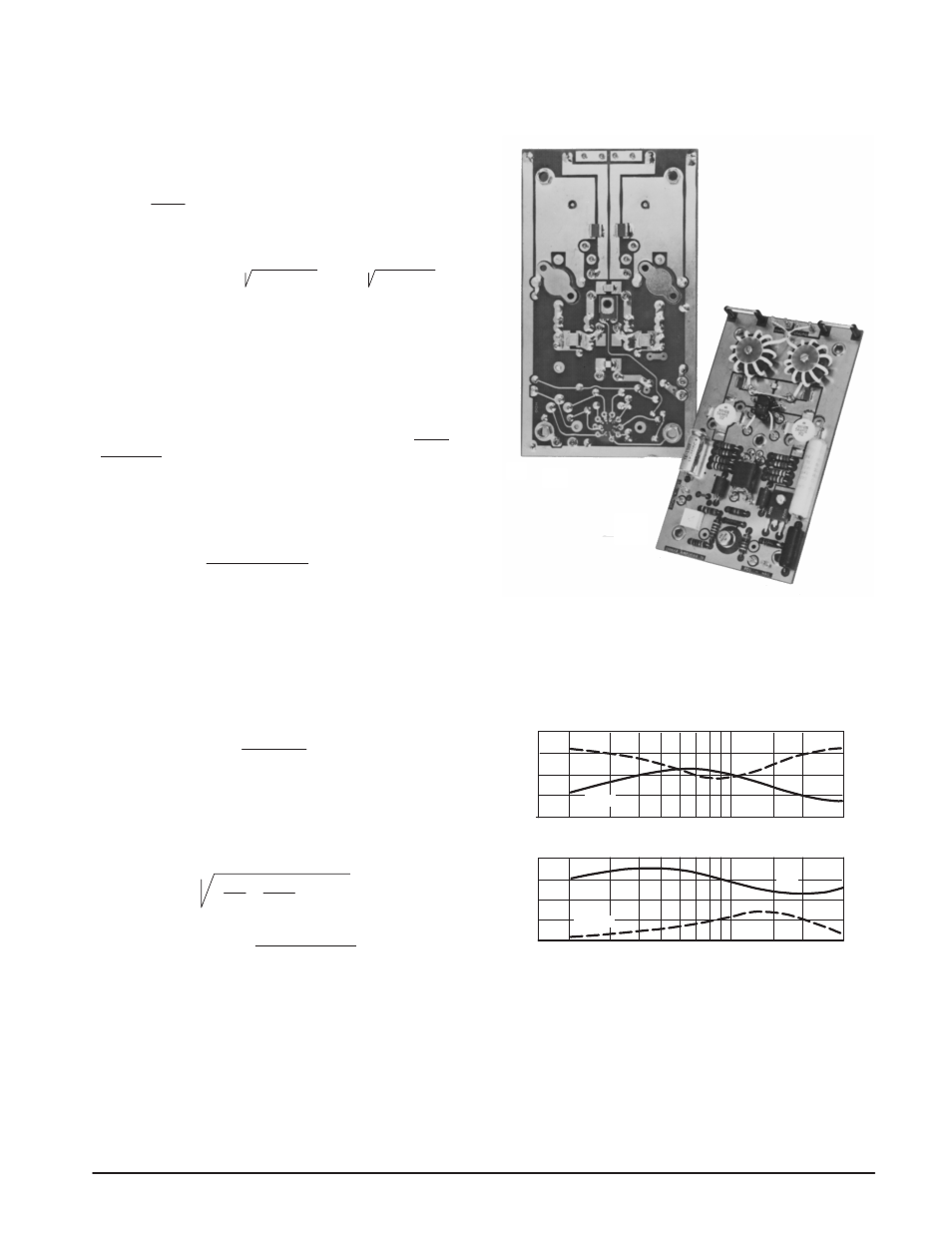
A photo of the circuit board is shown in Figure 5, A-bottom
and B-top. The performance data of the 300 W module can
be seen in Figure 6.
A.
B.
Figure 5. Bottom and Top of the 300 W Module
Circuit Board
IMD, d3 (dB)
η
(%)
50
40
30
30
35
40
IMD
G
PE
VSWR
η
FREQUENCY (MHz)
V
CC
= 50 V, P
out
= 300 W PEP
POWER GAIN (dB)
INPUT
VSWR
17
15
14
13
16
3.0
2.0
1.0
30
20
15
10
1.5 2.0
3.0
5.0
7.0
Figure 6. IMD, Power Gain, Input VSWR and Efficiency
versus Frequency of a 300 W Module
THE DRIVER AMPLIFIER
The driver uses a pair of MRF427 devices, and the same
circuit board layout as the power amplifier, with the exception
of the type of the output transformer.