Communication Concepts AN779 Application Note User Manual
Low-distortion 1.6 to 30 mhz ssb driver designs, Semiconductor, An779

AR
C
HIVE INF
O
RMA
TI
O
N
PRODUCT TRANSFERRED T
O
M/A–COM
1
RF Application Reports
LOW-DISTORTION 1.6 TO 30 MHz SSB DRIVER DESIGNS
Prepared by: Helge O. Granberg
RF Circuits Engineering
GENERAL CONSIDERATION
Two of the most important factors to be considered in
broadband linear amplifier design are the distortion and the
output harmonic rejection.
The major cause for intermodulation distortion is
amplitude nonlinearity in the active element. The nonlinearity
generates harmonics, and the fundamental odd-order
products are defined as 2
f1–f2
, 2
f2–f1
, 3
f2
– 2
f2
, 3
f2
– 2
f1
, etc.,
when a two-tone test signal is used. These harmonics may
not always appear in the amplifier output due to filtering and
cancellation effects, but are generated within the active
device. The amplitude and harmonic distortion cannot really
be distinguished, except in a case of a cascaded system,
where even-order products in each stage can produce
odd-order products through mixing processes that fall in the
fundamental region.
2
This, combined with phase distortion
— which in practical circuits is more apparent at higher
frequencies — can make the distortion analysis extremely
difficult;
5,2
whereas, if only amplitude distortion was present,
the effect of IMD in each stage could easily be calculated.
In order to expect a low harmonic output of the power
amplifier, it is also important for the driving source to be
harmonic-free. This is difficult in a four-octave bandwidth
system, even at 10 – 20 watt power levels. Class A biasing
helps the situation, and Class A push-pull yields even better
results due to the automatic rejection of even harmonics.
Depending on the application, a full Class A system is
not always feasible because of its low efficiency. The
theoretical maximum is 50%, but practical figures are not
higher than 25% to 35%. It is sometimes advantageous to
select a bias point somewhere between Class AB and A
which would give sufficiently good results, since filtering is
required in the power amplifier output in most instances
anyway.
In order to withstand the high level of steady dc bias
current, Class A requires a much larger transistor die than
Class B or AB for a specific power output. There are
sophisticated methods such as generating the bias voltage
from rectified RF input power, making the dc bias proportional
to the drive level.
1
This also yields to a better efficiency.
20 W, 25 dB AMPLIFIER WITH LOW-COST
PLASTIC DEVICES
The amplifier described here provides a total power gain
of about 25 dB, and the construction technique allows the
use of inexpensive components throughout. The plastic RF
power transistors, MRF475 and MRF476, featured in this
amplifier, were initially developed for the CB market. The high
manufacturing volume of these TO-220 packaged parts
makes them ideal for applications up to 50 MHz, where low
cost is an important factor.
The MRF476 is specified as a 3-watt device and the
MRF475 has an output power of 12 watts. Both are extremely
tolerant to overdrive and load mismatches, even under CW
conditions. Typical IMD numbers are better than -35 dB, and
power gains are 18 dB and 12 dB, respectively, at 30 MHz.
The collectors of the transistors are electrically connected
to the TO-220 package mounting tab which must be isolated
from the ground with proper mounting hardware (TO-220 AB)
or by floating heat dissipators. The latter method, employing
Thermalloy 6107 and 6106 heat dissipators, was adapted
for this design. Without an airflow, the 6106 and 6107 provide
sufficient heat sinking for about 30% duty cycle in the CW
mode. Collector idle currents of 20 mA are recommended
for both devices, but they were increased to 100 mA for the
MRF475 and to 40 mA for the MRF476 to reduce the higher
order IMD products and to achieve better harmonic
suppression.
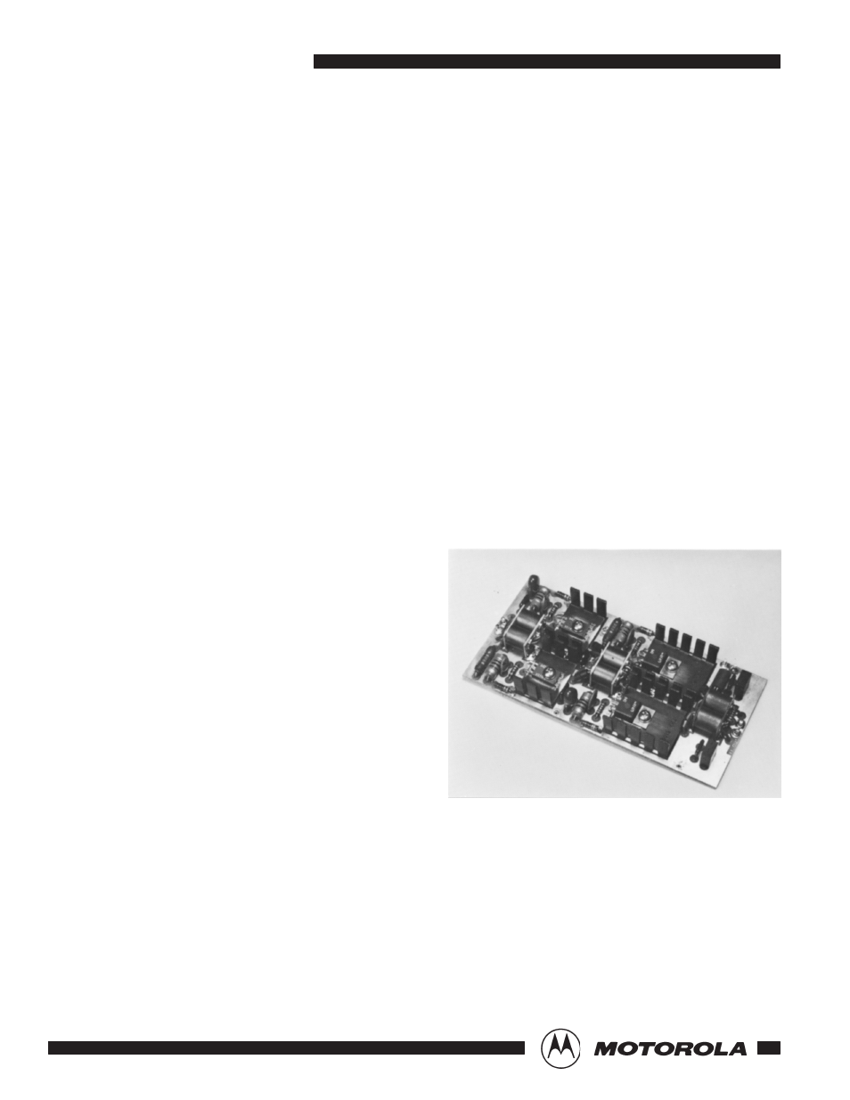
Figure 1.
Biasing and Feedback
The biasing is achieved with the well-known clamping
diode arrangement (Figure 2). Each stage has it own diode,
resistor, and bypass network, and the diodes are mounted
between the heat dissipators, being in physical contact with
them for temperature-tracking purposes. A better thermal
contact is achieved through the use of silicone grease in
these junctions.
The bias currents of each stage are individually adjustable
with R5 and R6. Capacitors C4 and C10 function as
audio-frequency bypasses to further reduce the source
impedance at the frequencies of modulation.
MOTOROLA
SEMICONDUCTOR
APPLICATION NOTE
Order this document
by AN779/D
Motorola, Inc. 1993
AN779
