Communication Concepts AN758 User Manual
Page 2
AR
C
HIVE INF
O
RMA
TI
O
N
PRODUCT TRANSFERRED T
O
M/A
–
COM
AN758
2
RF Application Reports
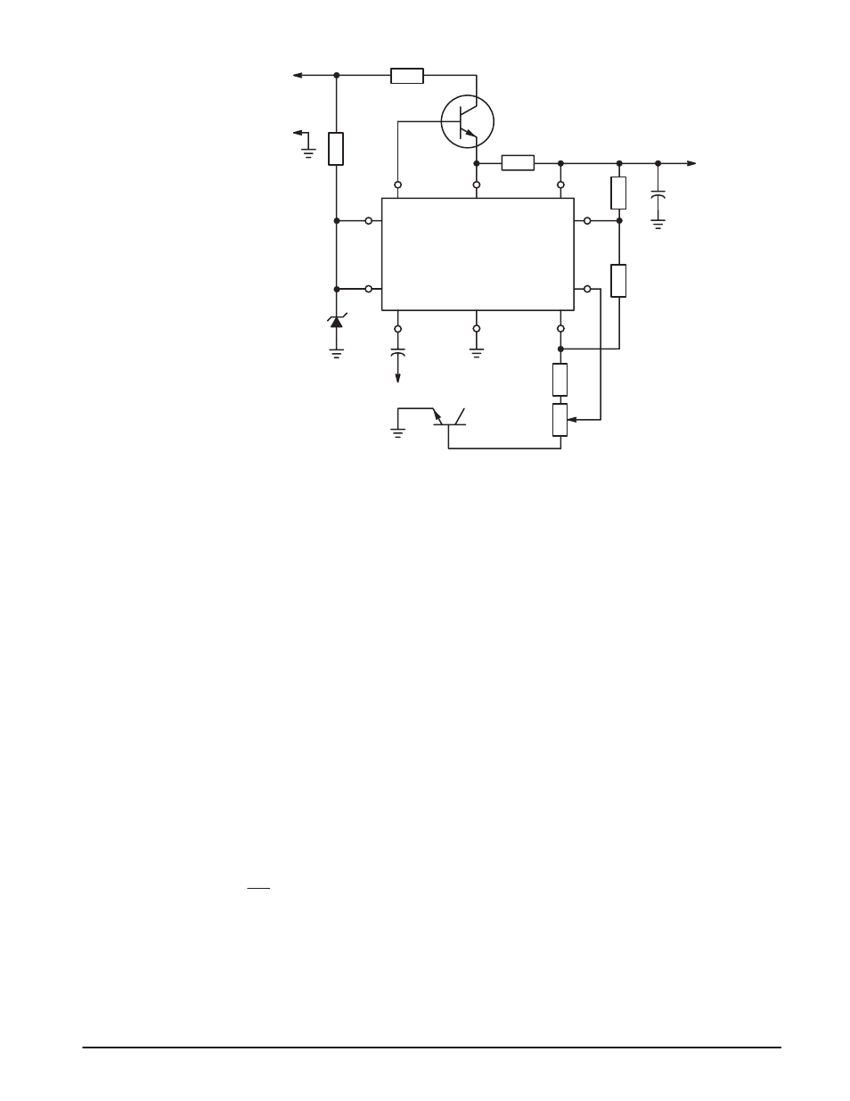
R9
+
50 V
-
R7
R12
R5
R6
R8
R10
C12
D2
D1
5
9
7
8
6
10
1
2
4
3
C13
+
-
BIAS OUT
+ 0.5 Ċ 1.0 V
TO PIN 2
Q3
MC1723C
Parts List:
R5
— 1.0 Ohm / 1/2 W
R6
— 1 k
Ω / 1/2 W
R7
— 100 Ohm/5 W
R8
— 18 k
Ω / 1/2 W
R9
— 8.2 k
Ω / 1/2 W
R10 — 1 k
Ω trimpot
R11 — ——————
R12 — 1 k
Ω / 1/2 W
C11 — 1000
µF / 3 V Electrolytic
C12 — 1000 pF Ceramic
D1
— See text
D2
— 1N5361 — 1N5366
Q3 — 2N5991
Figure 1. Bias Voltage Source
Although the MC1723C is specified for a minimum V
O
of 2 Volts, it can be used at lower levels with relaxed
specifications, which are sufficient for this application.
Advantages of this type bias source are:
1. Line voltage regulation, which is important if the amplifier
is to be operated from various supply voltages.
2. Adjustable current limit.
3. Very low stand-by current drain.
Figure 1 is modified from the circuit shown on the MC1723
data sheet by adding the temperature sensing diode D1 and
the voltage adjust element R10. D2 and R12 reduce the
supply voltage to a level below 40 V, which is the maximum
input voltage of the regulator.
D1 is the base-emitter junction of a 2N5190, in a Case
77 plastic package. The outline dimensions allow its use for
one of the circuit board stand-offs, attaching it automatically
to the heatsink for temperature tracking.
The temperature compensation has a slight negative
coefficient. When the collector idling current is adjusted to
300 mA at 25
°C, it will be reduced to 240 – 260 mA at a
60
°C heatsink temperature. (– 1.15 to – 1.7 mA/°C.)
The current limiting resistor R5 sets the limiting to
approximately 0.65 A, which is sufficient for devices with
a minimum h
FE
of 17,
I
B
=
h
FE
I
C
when the maximum average I
C
is 10.9 A.(2 MHz, 50 V,
250 CW.) Typically, the MRF428 h
FE
’s are in the 30’s.
The measured output voltage variations of the bias source
(0 – 600 mA) are
± 5 to 7 mV, which amounts to a source
impedance of approximately 20 milliohms.
THE 300 W AMPLIFIER MODULE
Input Matching
Due to the large emitter periphery of the MRF428, the
series base impedance is as low as 0.88, – J.80 Ohm at
30 MHz. In a push-pull circuit a 16:1 input transformer would
provide the best impedance match from a 50-Ohm source.
This would however, result in a high VSWR at 2 MHz, and
would make it difficult to implement the gain correction
network design. For this reason a 9:1 transformer, which is
more ideal at the lower frequencies, was chosen. This
represents a 5.55 Ohm base-to-base source impedance.
In a Class C push-pull circuit, where the conduction angle
is less than 180
°, the base-to-base impedance would be
about four times the base-to-emitter impedance of one
device. In Class A where the collector idling current is
approximately half the peak collector current, the conduction
angle is 360
°, and the base-to-base impedance is twice the
input impedance of one transistor. When the forward base
bias is applied, the conduction angle increases and the
base-to-base impedance decreases rapidly, approaching
that of Class A in Class AB.
A center tap, common in push-pull circuits, is not
necessary in the input transformer secondary, if the
transistors are balanced. (C
ib
, h
FE
, V
BEf
) The base current
return path is through the forward biased base-emitter
junction of the off transistor. This junction acts as a clamping
diode, and the power gain is somewhat dependent upon the
amount of the bias current. The equivalent input circuit
(Figure 2) represents one half of the push-pull circuit, and
for calculations R
S
equals the total source impedance (R
S
′
)
divided by two.