Communication Concepts AN758 User Manual
Page 4
AR
C
HIVE INF
O
RMA
TI
O
N
PRODUCT TRANSFERRED T
O
M/A
–
COM
AN758
4
RF Application Reports
+
50 V
-
R2
R1
L5
TO BIAS
SOURCE
Q1
Q2
R3
R4
C5
e
f
a
c
b
d
C4
C1
C3
T1
INPUT
50 Ω
L1
L2
C2
L9
L3
C11
C10
C8
C6
C7
T2
+
-
OUTPUT
50 Ω
a
b
T3
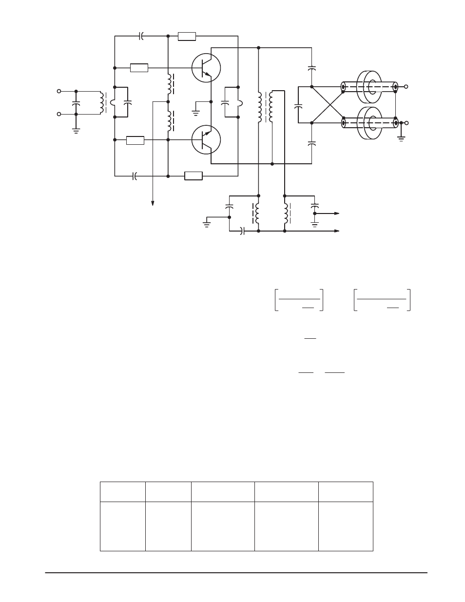
Figure 3.
In addition to providing a source for the negative
feedback, T2 supplies the dc voltage to the collectors as well
as functions as a center tap for the output transformer T3.
The currents for each half cycle are in opposite phase
in ac and bd, and depending on the coupling factor between
the windings, the even harmonic components will see a much
lower impedance than the fundamental. The optimum line
i m p e d a n c e f o r a c , b d w o u l d e q u a l o n e h a l f t h e
collector-to-collector impedance, but experiments have
shown that increasing this number by a factor of 2–3 affects
the 2nd and 4th harmonic amplitudes by only 1 to 2 dB.
Since the minimum gain loss obtainable at 30 MHz with
network as in Figure 2, and the modified VCS2 source was
about 3.8 dB at 30 MHz, C5 was added with the following
in mind: C5 and L5 form a parallel resonant circuit with a
Q of approximately 1.5. Its purpose is to increase the
shunting impedance across the bases, and to disturb the
180
° phase difference between the input signal and the
feedback voltage at the higher frequencies. This reduces the
gain loss of 3.8 dB, of which 1.4 dB is caused by the feedback
at 30 MHz. The amount depends upon the resonant
frequency of C5 L5, which should be above the highest
operating frequency, to avoid possible instabilities.
When L5 is 45 nH, and the resonance is calculated for
35 MHz, the value of C5 becomes 460 pF, which can be
rounded to the closest standard, or 470 pF. The phase shift
at 30 MHz is:
6.8 1 –
6.28 x 30 x 0.045
1225
900
Ǔ
ǒ
Tan
–1
=
R 1 –
2
πfL
f
o
2
f
2
Ǔ
ǒ
Tan
–1
= 78.0
°
1.80
8.48
Ǔ
ǒ
Tan
–1
=
The impedance is:
cos
θ
R
=
cos 78
°
6.8
= 32.7
Ω
At 2 MHz the numbers are respectively 4.76
° and 6.83 Ω.
The 1.4 dB feedback means that the feedback voltage
is 16% of the input voltage at the bases. By the aid of vectors,
we can calculate that the 78
° phase shift and the increased
impedance reduces this to 4%, which amounts to 0.35 dB.
These numbers were verified in another computer program
with VCS2 = 6.9 V, and including C5. New values for R1
and R2 were obtained as 1.95
Ω and 6.8 Ω respectively,
and other data as shown in Table 1.
Table 1.
Frequency
MHz
Input
VSWR
Input Impedance
Real
Input Impedance
Reactive
Attenuation
dB
2.0
1.07
2.79
– 0.201
13.00
4.0
1.16
2.66
– 0.393
12.07
7.5
1.33
2.35
– 0.615
10.42
15
1.68
1.77
– 0.611
7.40
20
1.82
1.57
– 0.431
5.90
30
1.74
1.62
– 0.21
2.70