Communication Concepts EB27A Engineering Bulletin User Manual
Archive informa tion archive informa tion, Semiconductor, Eb27a
ARCHIVE INFORMA
TION
ARCHIVE INFORMA
TION
1
RF Application Reports
GET 300 WATTS PEP LINEAR ACROSS 2 TO 30 MHz
FROM THIS PUSH-PULL AMPLIFIER
Prepared by: Helge Granberg
Circuits Engineer, SSB
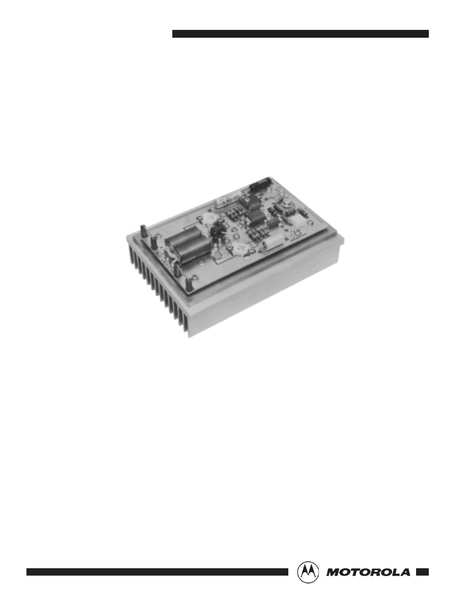
(The heat sink shown with amplifier is sufficient only for short test periods under forced air cooling.)
This bulletin supplies sufficient information to build a
push-pull linear amplifier for 300 watts of PEP or CW output
power across the 2- to 30-MHz band. One of Motorola’s new
high-power transistors developed for single-sideband,
MRF422, is used in this application.
Like all transistors in its family of devices, MRF422
combines single-chip construction that is advancing the
state-of-the-art, and improved packaging to accommodate
the low collector efficiencies encountered in class B
operation. Rated maximum output power is 150 watts CW
or PEP with intermodulation distortion spec’d at – 30 dB
maximum, – 33 dB typical. Although not recommended, a
saturated power level of 240- to 250-W is achievable.
Maximum allowable dissipation is 300 W at 25
°
C.
Because of its excellent load and line voltage regulating
capabilities, an integrated circuit bias regulator is used in the
amplifier. The MPC1000, originally described in this bulletin,
consisted of a MC1723 chip and a built-in pass transistor.
The manufacture of this device has been discontinued
however, and the board lay-out was modified to incorporate
the above two in separate packages. The load regulation
typically measures less than 2% at current levels up to 0.5
A, which assumes an h
FE
of 40 for the RF power devices.
The board surface provides a sufficient heat sink for the
2N5990 pass transistor, but a separate heat dissipator, such
as Thermalloy 6107 can be added if necessary. With the
component values shown, the bias is adjustable from 0.4
to 0.8 volts.
Gain flatness over the band is achieved using base input
networks R
1
C
2
and R
2
C
3
and negative feedback through R
3
and R
4
. The networks represent a series reactance of 0.69
ohms at 30 MHz rising to 1.48 ohms at 2 MHz. A single-turn
winding in the collector choke provides a low-impedance
negative feedback source, thus R
3
and R
4
determine the
amount. The reactance of C
4
reduces feedback at high
frequencies with the result that feedback increases an
average of 4 dB per octave at decreasing frequency.
MOTOROLA
SEMICONDUCTOR
Order this document
by EB27A/D
ENGINEERING BULLETIN
Motorola, Inc. 1993
EB27A