Zxld1366, Device description – Diodes ZXLD1366 User Manual
Page 6
ZXLD1366
Document number: DS31992 Rev. 8 - 2
2 of 30
October 2013
© Diodes Incorporated
A Product Line of
Diodes Incorporated
ZXLD1366
Device Description
(cont.)
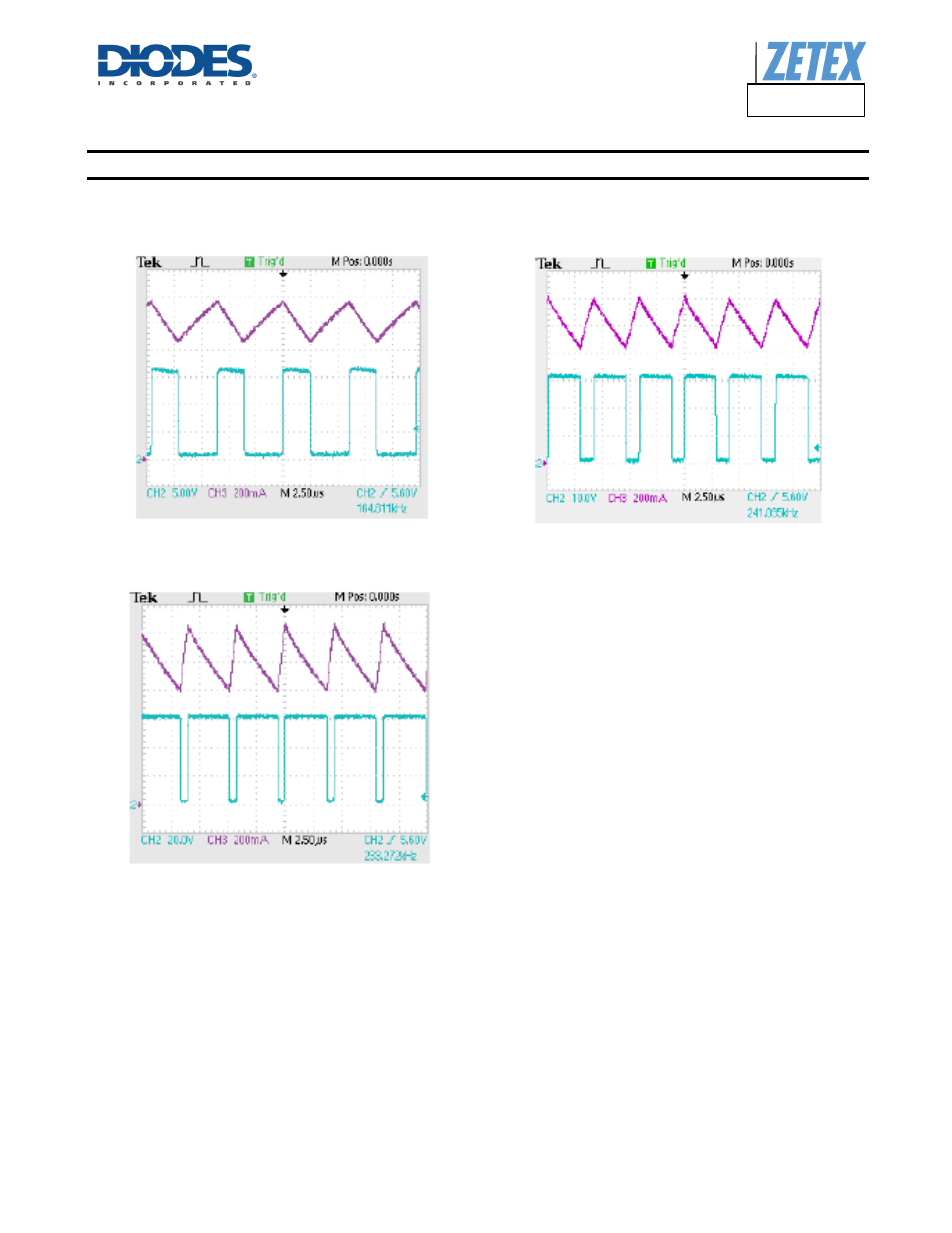
Actual operating waveforms
V
IN
= 15V, R
S
= 0.2
Ω, L = 68µH
Normal operation.
Output Current (Ch 3) and LX voltage (Ch 2)
V
IN
= 30V, R
S
= 0.2
Ω, L = 68µH
Normal operation.
Output Current (Ch 3) and LX voltage (Ch 2)
V
IN
= 60V, R
S
= 0.2
Ω, L = 68µH
Normal operation.
Output Current (Ch 3) and LX voltage (Ch 2)
Adjusting Output Current
The device contains a low pass filter between the ADJ pin and the threshold comparator and an internal current limiting resistor (50kΩ nom)
between ADJ and the internal reference voltage. This allows the ADJ pin to be overdriven with either DC or pulse signals to change the
V
SENSE
switching threshold and adjust the output current.
Details of the different modes of adjusting output current are given in the applications section.
Output Shutdown
The output of the low pass filter drives the shutdown circuit. When the input voltage to this circuit falls below the threshold (0.2V nom.), the
internal regulator and the output switch are turned off. The voltage reference remains powered during shutdown to provide the bias current
for the shutdown circuit. Quiescent supply current during shutdown is nominally 60μA and switch leakage is below 5μA.