Zxld1366, Application information – Diodes ZXLD1366 User Manual
Page 18
ZXLD1366
Document number: DS31992 Rev. 8 - 2
18 of 30
October 2013
© Diodes Incorporated
A Product Line of
Diodes Incorporated
ZXLD1366
Application Information
(cont.)
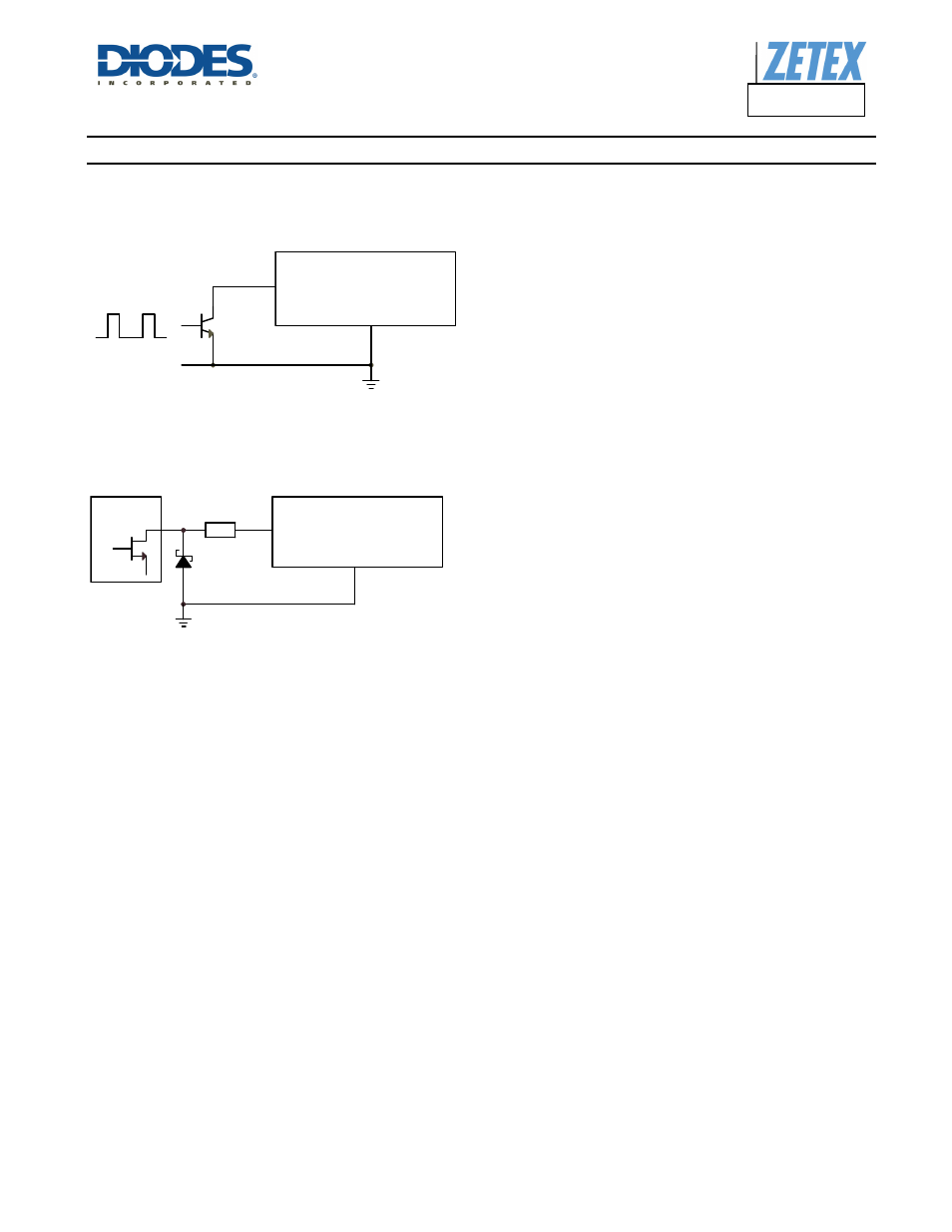
Driving the ADJ Input via Open Collector Transistor
The recommended method of driving the ADJ pin and controlling the amplitude of the PWM waveform is to use a small NPN switching
transistor as shown below:
This scheme uses the 50k resistor between the ADJ pin and the internal voltage reference as a pull-up resistor for the external transistor.
Driving the ADJ Input from a Microcontroller
Another possibility is to drive the device from the open drain output of a microcontroller. The diagram below shows one method of doing this:
If the NMOS transistor within the microcontroller has high Gate / Drain capacitance, this arrangement can inject a negative spike into ADJ
input of the ZXLD1366 and cause erratic operation but the addition of a Schottky clamp diode (eg Diodes Inc. SD103CWS) to ground and
inclusion of a series resistor (3.3k) will prevent this. See the section on PWM dimming for more details of the various modes of control using
high frequency and low frequency PWM signals.
Shutdown Mode
Taking the ADJ pin to a voltage below 0.2V for more than approximately 100μs will turn off the output and supply current to a low standby level
of 65μA nominal.
Note that the ADJ pin is not a logic input. Taking the ADJ pin to a voltage above V
REF
will increase output current above the 100% nominal
average value. (See page 18 graphs for details).
PWM
GND
ZXLD1366
ADJ
GND
GND
ZXLD1366
ADJ
MCU
3.3k