Block diagram, Pin description, Zxld1366 – Diodes ZXLD1366 User Manual
Page 2
ZXLD1366
Document number: DS31992 Rev. 8 - 2
2 of 30
October 2013
© Diodes Incorporated
A Product Line of
Diodes Incorporated
ZXLD1366
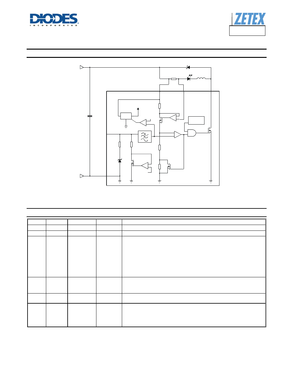
Block Diagram
Figure. 1 Pin Connection for TSOT25 Package
Pin Description
Name TSOT25 U-DFN3030-6 SO-8EP
Function
LX
1
1
1
Drain of NDMOS switch
GND
2
2, 5
2, 3, 6, 7
Ground (0V)
ADJ 3
3 4
Multi-function On/Off and brightness control pin:
•
Leave floating for normal operation.(V
ADJ
= V
REF
= 1.25V giving nominal
average output current I
OUTnom
= 0.2V/
RS
)
•
Drive to voltage below 0.2V to turn off output current
•
Drive with DC voltage (0.3V < V
ADJ
< 2.5V) to adjust output current from 25%
to 200% of I
OUTnom
•
Connect a capacitor from this pin to ground to set soft-start time.
Soft start time increases approximately 0.2ms/nF
I
SENSE
4
4 5
Connect resistor RS from this pin to VIN to define nominal average output current
I
OUTnom
= 0.2V
/RS
.
(Note: R
SMIN
= 0.2V with ADJ pin open-circuit)
V
IN
5 6 8
Input Voltage (6V to 60V). Decouple to ground with 4.7µF of higher X7R ceramic
capacitor close to device.
Pad -
Pad Pad
Exposed Pad (EP) - connected to device substrate.
To improve thermal impedance of package the EP must be connected to power
ground but should not be used as the 0V (GND) current path.
It can be left floating but must not be connected to any other voltage other than
0V.
Low voltage
detector
Voltage
regulator
LX
MN
L1
D1
I
SENSE
Adj
Gnd
V
IN
V
IN
50K
20K
1.25V
1.35V
0.2V
600KHz
+
-
+
-
+
-
R4
R5
R2
R3
R1
2
3
5
4
1
D1
+
-
R
S
C1
4.7µF
5V