Device description, Zxld1366 – Diodes ZXLD1366 User Manual
Page 5
ZXLD1366
Document number: DS31992 Rev. 8 - 2
5 of 30
October 2013
© Diodes Incorporated
A Product Line of
Diodes Incorporated
ZXLD1366
Device Description
The device, in conjunction with the coil (L1) and current sense resistor (R
S
), forms a self-oscillating continuous-mode buck converter.
Device Operation
(refer to Figure 1 - Block diagram and Figure 2 Operating waveforms).
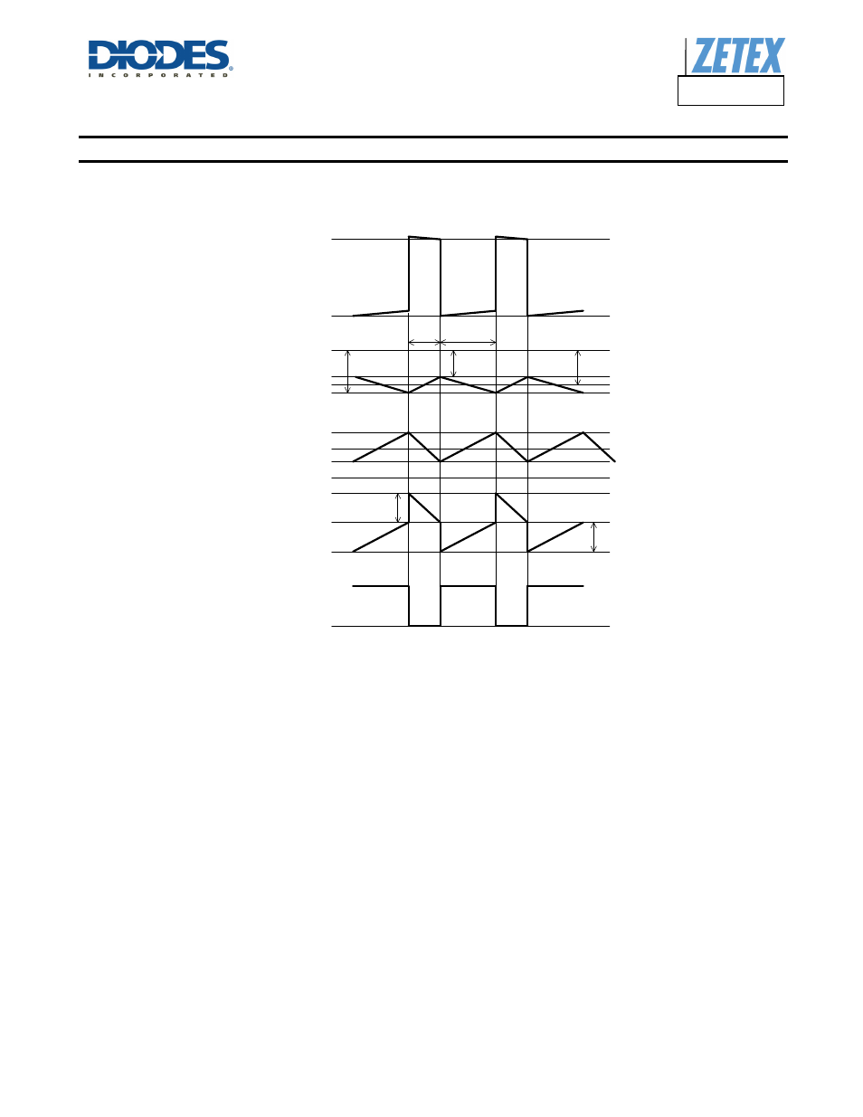
Figure 2 Theoretical Operating Waveforms
Operation can be best understood by assuming that the ADJ pin of the device is unconnected and the voltage on this pin (V
ADJ
) appears
directly at the (+) input of the comparator.
When input voltage V
IN
is first applied, the initial current in L1 and R
S
is zero and there is no output from the current sense circuit. Under this
condition, the (-) input to the comparator is at ground and its output is high. This turns MN on and switches the LX pin low, causing current to
flow from V
IN
to ground, via R
S
, L1 and the LED(s). The current rises at a rate determined by V
IN
and L1 to produce a voltage ramp (V
SENSE
)
across R
S
. The supply referred voltage V
SENSE
is forced across internal resistor R1 by the current sense circuit and produces a proportional
current in internal resistors R2 and R3. This produces a ground referred rising voltage at the (-) input of the comparator. When this reaches
the threshold voltage (V
ADJ
), the comparator output switches low and MN turns off. The comparator output also drives another NMOS switch,
which bypasses internal resistor R3 to provide a controlled amount of hysteresis. The hysteresis is set by R3 to be nominally 15% of V
ADJ
.
When MN is off, the current in L1 continues to flow via D1 and the LED(s) back to V
IN
. The current decays at a rate determined by the LED(s)
and diode forward voltages to produce a falling voltage at the input of the comparator. When this voltage returns to V
ADJ
, the comparator
output switches high again. This cycle of events repeats, with the comparator input ramping between limits of V
ADJ
± 15%.
Switching Thresholds
With V
ADJ
= V
REF
, the ratios of R1, R2 and R3 define an average V
SENSE
switching threshold of 200mV (measured on the I
SENSE
pin with
respect to V
IN
). The average output current I
OUTnom
is then defined by this voltage and R
S
according to:
I
OUTnom
= 200mV/R
S
Nominal ripple current is ±30mV/R
S
0V
V
IN
200mV
230mV
0V
SENSE voltage
V
SENSE+
V
SENSE-
Toff
Ton
170mV
0V
5V
V
IN
0.15V
ADJ
0.15V
ADJ
I
OUTnom
I
OUTnom
+15%
I
OUTnom
-15%
V
ADJ
LX voltage
Coil current
Comparator
input voltage
Comparator
output