Zxld1366, Application information – Diodes ZXLD1366 User Manual
Page 26
ZXLD1366
Document number: DS31992 Rev. 8 - 2
26 of 30
October 2013
© Diodes Incorporated
A Product Line of
Diodes Incorporated
ZXLD1366
Application Information
(cont.)
High Voltage Tracks
Avoid running any high voltage tracks close to the ADJ pin, to reduce the risk of leakage currents due to board contamination. The ADJ pin is
soft-clamped for voltages above 1.35V to desensitize it to leakage that might raise the ADJ pin voltage and cause excessive output current.
However, a ground ring placed around the ADJ pin is recommended to minimize changes in output current under these conditions.
Evaluation PCB
ZXLD1366 evaluation boards are available on request. Terminals allow users to interface the boards to their preferred LED products.
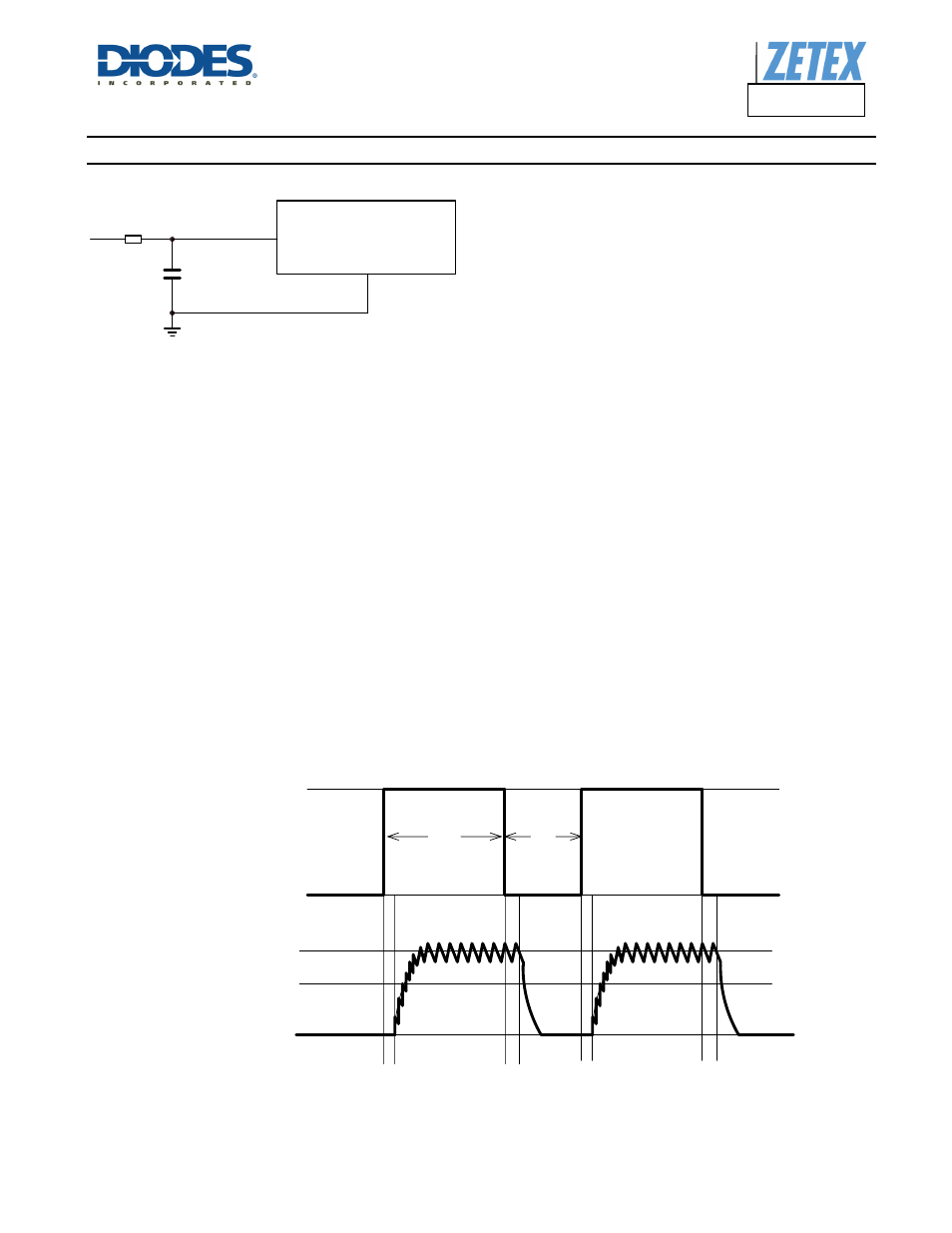
Dimming Output Current Using PWM
Low Frequency PWM Mode
When the ADJ pin is driven with a low frequency PWM signal (eg 100Hz), with a high level voltage V
ADJ
and a low level of zero, the output of
the internal low pass filter will swing between 0V and V
ADJ
, causing the input to the shutdown circuit to fall below its turn-off threshold (200mV
nom) when the ADJ pin is low. This will cause the output current to be switched on and off at the PWM frequency, resulting in an average
output current I
OUTavg
proportional to the PWM duty cycle.
(See Figure 9 - Low frequency PWM operating waveforms).
The average value of output current in this mode is given by:
I
OUTavg
0.2D
PWM
/R
S
[for D
PWM
>0.001]
This mode is preferable if optimum LED 'whiteness' is required. It will also provide the widest possible dimming range (approx. 1000:1) and
higher efficiency at the expense of greater output ripple.
Figure 9 Low Frequency PWM Operating Waveforms
GND
ZXLD1366
ADJ
3.3k
100nF
GND
V
ADJ
PWM Voltage
Ton
IOUTavg
0V
0
Toff
0.2/Rs
IOUTnom
Output Current