Zxld1366, Application information – Diodes ZXLD1366 User Manual
Page 25
ZXLD1366
Document number: DS31992 Rev. 8 - 2
25 of 30
October 2013
© Diodes Incorporated
A Product Line of
Diodes Incorporated
ZXLD1366
Application Information
(cont.)
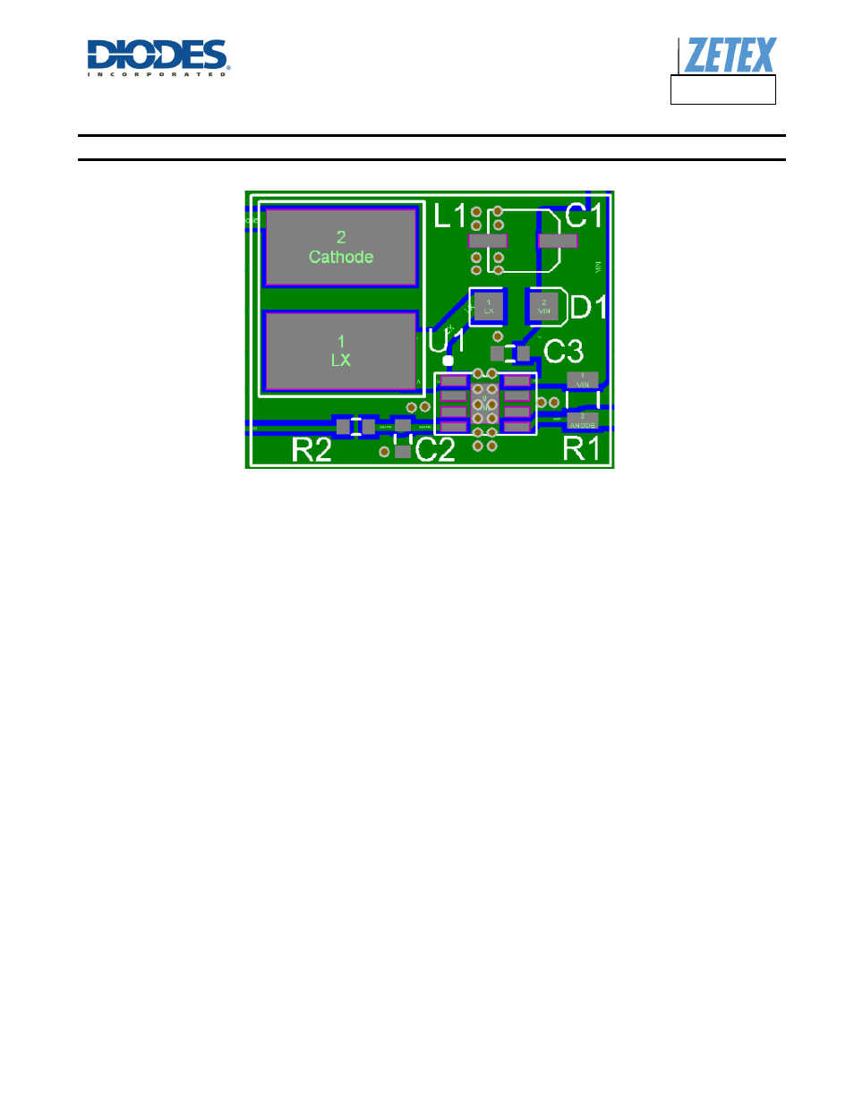
Figure 8 Suggested Layout for SO-8EP Package
Vias ensure an effective path to the ground plane for the heat flow therefore reducing the thermal impedance between junction and ambient
temperature. Diodes came to the conclusion that the compromise is reached by using more than 10 vias with 1mm of diameter and 0.5 hole
size.
Finally the same scheme in Figure 7 (without the exposed paddle) can be usde for the TSOT25 package guaranteeing an effective thermal
path.
Thermal Compensation of Output Current
High luminance LEDs often need to be supplied with a temperature compensated current in order to maintain stable and reliable operation at
all drive levels. The LEDs are usually mounted remotely from the device so, for this reason, the temperature coefficients of the internal circuits
for the ZXLD1366 have been optimized to minimize the change in output current when no compensation is employed. If output current
compensation is required, it is possible to use an external temperature sensing network normally using Negative Temperature Coefficient
(NTC) thermistors and/or diodes, mounted very close to the LED(s). The output of the sensing network can be used to drive the ADJ pin in
order to reduce output current with increasing temperature.
Layout Considerations
LX Pin
The LX pin of the device is a fast switching node, so PCB tracks should be kept as short as possible. To minimize ground 'bounce', the ground
pin of the device should be soldered directly to the ground plane.
Coil and Decoupling Capacitors and Current Sense Resistor
It is particularly important to mount the coil and the input decoupling capacitor as close to the device pins as possible to minimize parasitic
resistance and inductance, which will degrade efficiency. It is also important to minimize any track resistance in series with current sense
resistor R
S
. Its best to connect V
IN
directly to one end of R
S
and I
SENSE
directly to the opposite end of R
S
with no other currents flowing in these
tracks. It is important that the cathode current of the Schottky diode does not flow in a track between R
S
and V
IN
as this may give an apparent
higher measure of current than is actual because of track resistance.
ADJ Pin
The ADJ pin is a high impedance input for voltages up to 1.35V so, when left floating, PCB tracks to this pin should be as short as possible to
reduce noise pickup. A 100nF capacitor from the ADJ pin to ground will reduce frequency modulation of the output under these conditions. An
additional series 3.3kΩ resistor can also be used when driving the ADJ pin from an external circuit (see next page). This resistor will provide
filtering for low frequency noise and provide protection against high voltage transients.