40a analog megadlynx, Non-isolated dc-dc power modules, Data sheet – GE Industrial Solutions 40A Analog MegaDLynx User Manual
Page 4: General specifications, Feature specifications
GE
Data Sheet
40A Analog MegaDLynx
TM
: Non-Isolated DC-DC Power Modules
4.5Vdc –14.4Vdc input; 0.6Vdc to 2.0Vdc output; 40A Output Current
April 24, 2013
©2012 General Electric Company. All rights reserved.
Page 4
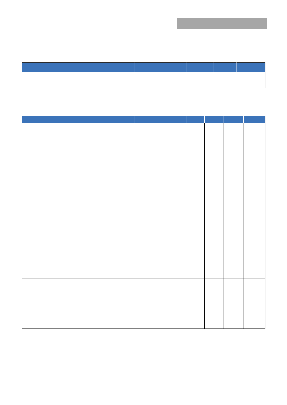
General Specifications
Parameter
Device
Min
Typ
Max
Unit
Calculated MTBF (I
O
=0.8I
O, max
, T
A
=40°C) Telecordia Issue 2 Method
1 Case 3
All
6,498,438
Hours
Weight
11.7 (0.41)
g (oz.)
Feature Specifications
Unless otherwise indicated, specifications apply over all operating input voltage, resistive load, and temperature conditions. See
Feature Descriptions for additional information.
Parameter
Device
Symbol
Min
Typ
Max
Unit
On/Off Signal Interface
(V
IN
=V
IN, min
to V
IN, max
; open collector or equivalent,
Signal referenced to GND)
Device is with suffix “4” – Positive Logic (See Ordering Information)
Logic High (Module ON)
Input High Current
All
I
IH
10
µA
Input High Voltage
All
V
IH
3.5
V
IN,max
V
Logic Low (Module OFF)
Input Low Current
All
I
IL
1
mA
Input Low Voltage
All
V
IL
-0.3
0.4
V
Device Code with no suffix – Negative Logic (See Ordering
Information)
(On/OFF pin is open collector/drain logic input with
external pull-up resistor; signal referenced to GND)
Logic High (Module OFF)
Input High Current
All
I
IH
―
―
1
mA
Input High Voltage
All
V
IH
2
―
V
IN, max
Vdc
Logic Low (Module ON)
Input low Current
All
I
IL
―
―
10
μA
Input Low Voltage
All
V
IL
-0.2
―
0.4
Vdc
Turn-On Delay and Rise Times
(V
IN
=V
IN, nom
, I
O
=I
O, max ,
V
O
to within ±1% of steady state)
Case 1: On/Off input is enabled and then input power is
applied (delay from instant at which V
IN
= V
IN, min
until V
o
=
10% of V
o, set
)
All
Tdelay
―
1.1
―
msec
Case 2: Input power is applied for at least one second and
then the On/Off input is enabled (delay from instant at
which Von/Off is enabled until V
o
= 10% of V
o, set
)
All
Tdelay
―
700
―
μsec
Output voltage Rise time (time for V
o
to rise from
10% of Vo, set to 90% of Vo, set)
All
Trise
―
1.5
―
msec
Output voltage overshoot (T
A
= 25
o
C
V
IN
= V
IN, min
to V
IN, max
,I
O
= I
O, min
to I
O, max
)
With or without maximum external capacitance
3.0
% V
O, set
Output voltage overshoot (T
A
= 25
o
C
V
IN
= V
IN, min
to V
IN, max
,I
O
= I
O, min
to I
O, max
)
With or without maximum external capacitance
3.0
% V
O, set