Picotlynx, 6a: non-isolated dc-dc power modules, Data sheet – GE Industrial Solutions PicoTLynx 6A User Manual
Page 15: Module
GE
Data Sheet
PicoTLynx
TM
6A: Non-Isolated DC-DC Power Modules
2.4Vdc –5.5Vdc input; 0.6Vdc to 3.63Vdc output; 6A Output Current
September 11, 2013
©2013 General Electric Company. All rights reserved.
Page 15
Output Voltage Sequencing
The APTH006A0X modules include a sequencing feature, EZ-
SEQUENCE that enables users to implement various types of
output voltage sequencing in their applications. This is
accomplished via an additional sequencing pin. When not using
the sequencing feature, either tie the SEQ pin to V
IN
or leave it
unconnected.
When an analog voltage is applied to the SEQ pin, the output
voltage tracks this voltage until the output reaches the set-point
voltage. The final value of the SEQ voltage must be set higher
than the set-point voltage of the module. The output voltage
follows the voltage on the SEQ pin on a one-to-one volt basis. By
connecting the SEQ pins of multiple modules together, all
modules can track their output voltages to the voltage applied
on the SEQ pin.
For proper voltage sequencing, first, input voltage is applied to
the module. The On/Off pin of the module is left unconnected (or
tied to GND for negative logic modules or tied to V
IN
for positive
logic modules) so that the module is ON by default. After
applying input voltage to the module, a minimum 10msec delay
is required before applying voltage on the SEQ pin. This delay
gives the module enough time to complete its internal power-up
soft-start cycle. During the delay time, the SEQ pin should be
held close to ground (nominally 50mV ± 20 mV). This is required
to keep the internal op-amp out of saturation thus preventing
output overshoot during the start of the sequencing ramp. By
selecting resistor R1 (see fig. 43) according to the following
equation
05
.
0
24950
1
−
=
IN
V
R
ohms,
the voltage at the sequencing pin will be 50mV when the
sequencing signal is at zero.
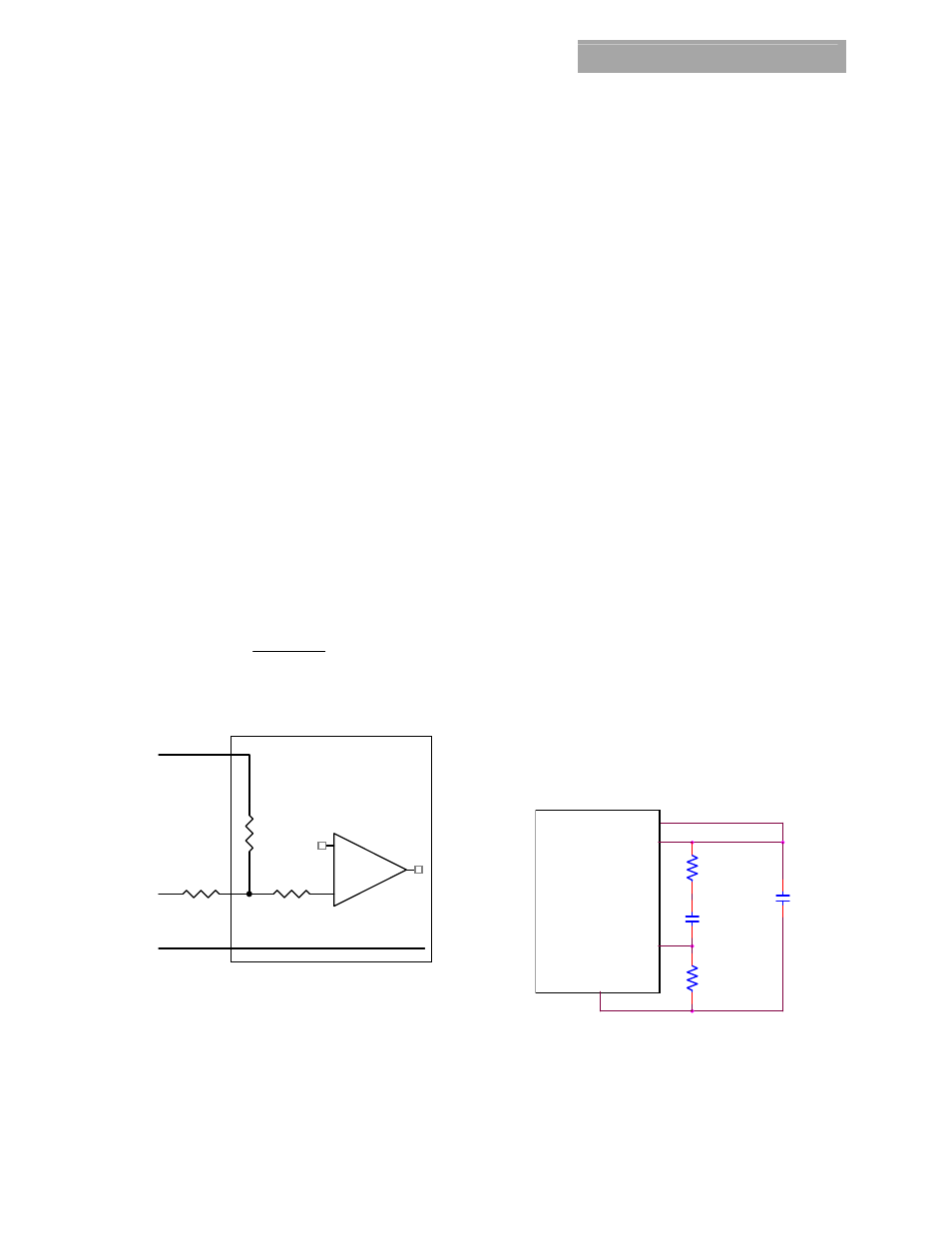
R1
GND
VIN+
SEQ
+
-
OUT
10K
499K
MODULE
Figure 43. Circuit showing connection of the sequencing
signal to the SEQ pin.
After the 10msec delay, an analog voltage is applied to the SEQ
pin and the output voltage of the module will track this voltage
on a one-to-one volt bases until the output reaches the set-
point voltage. To initiate simultaneous shutdown of the
modules, the SEQ pin voltage is lowered in a controlled manner.
The output voltage of the modules tracks the voltages below
their set-point voltages on a one-to-one basis. A valid input
voltage must be maintained until the tracking and output
voltages reach ground potential.
When using the EZ-SEQUENCE
TM
feature to control start-up of
the module, pre-bias immunity during start-up is disabled. The
pre-bias immunity feature of the module relies on the module
being in the diode-mode during start-up. When using the EZ-
SEQUENCE
TM
feature, modules goes through an internal set-up
time of 10msec, and will be in synchronous rectification mode
when the voltage at the SEQ pin is applied. This will result in the
module sinking current if a pre-bias voltage is present at the
output of the module. When pre-bias immunity during start-up
is required, the EZ-SEQUENCE
TM
feature must be disabled. For
additional guidelines on using the EZ-SEQUENCE
TM
feature
please refer to Application Note AN04-008 “Application
Guidelines for Non-Isolated Converters: Guidelines for
Sequencing of Multiple Modules”, or contact the Lineage Power
technical representative for additional information.
Tunable Loop
TM
The 5V Pico TLynx
TM
6A modules have a new feature that
optimizes transient response of the module called Tunable
Loop
TM
.
External capacitors are usually added to the output of the
module for two reasons: to reduce output ripple and noise (see
Figures 36 and 37) and to reduce output voltage deviations
from the steady-state value in the presence of dynamic load
current changes. Adding external capacitance however affects
the voltage control loop of the module, typically causing the
loop to slow down with sluggish response. Larger values of
external capacitance could also cause the module to become
unstable.
The Tunable Loop
TM
allows the user to externally adjust the
voltage control loop to match the filter network connected to
the output of the module. The Tunable Loop
TM
is implemented by
connecting a series R-C between the SENSE and TRIM pins of the
module, as shown in Fig. 44. This R-C allows the user to
externally adjust the voltage loop feedback compensation of the
module.
MODULE
VOUT
SENSE
TRIM
GND
RTUNE
CTUNE
RTrim
C O
Figure. 44. Circuit diagram showing connection of R
TUME
and
C
TUNE
to tune the control loop of the module.
Recommended values of R
TUNE
and C
TUNE
for different output
capacitor combinations are given in Tables 2, 3, 4 and 5. Tables
2 and 4 shows the recommended values of R
TUNE
and C
TUNE
for
different values of ceramic output capacitors up to 940uF that