Test configurations, Design considerations, Tlynx – GE Industrial Solutions TLynx User Manual
Page 11: Input filtering
Data Sheet
August 13, 2013
TLynx
TM
: Non-isolated DC-DC Power Modules:
2.4 – 5.5Vdc input; 0.6Vdc to 3.63Vdc output; 20A output current
LINEAGE
POWER
11
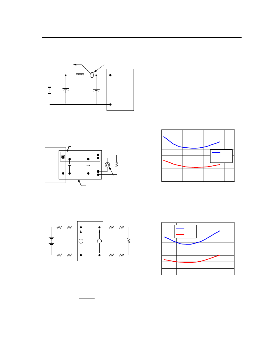
Test Configurations
TO OSCILLOSCOPE
CURRENT PROBE
L
TEST
1μH
BAT
T
E
R
Y
C
S
1000μF
Electrolytic
E.S.R.<0.1
Ω
@ 20°C 100kHz
2x100μF
Tantalum
V
IN
(+)
COM
NOTE: Measure input reflected ripple current with a simulated
source inductance (L
TEST
) of 1μH. Capacitor C
S
offsets
possible battery impedance. Measure current as shown
above.
C
IN
Figure 31. Input Reflected Ripple Current Test
Setup.
NOTE: All voltage measurements to be taken at the module
terminals, as shown above. If sockets are used then
Kelvin connections are required at the module terminals
to avoid measurement errors due to socket contact
resistance.
Vo+
COM
0.1uF
RESISTIVE
LOAD
SCOPE USING
BNC SOCKET
COPPER STRIP
GROUND PLANE
10uF
Figure 32. Output Ripple and Noise Test Setup.
V
O
COM
V
IN
(+)
COM
R
LOAD
R
contact
R
distribution
R
contact
R
distribution
R
contact
R
contact
R
distribution
R
distribution
V
IN
V
O
NOTE: All voltage measurements to be taken at the module
terminals, as shown above. If sockets are used then
Kelvin connections are required at the module terminals
to avoid measurement errors due to socket contact
resistance.
Figure 33. Output Voltage and Efficiency Test Setup.
η =
V
O
. I
O
V
IN
. I
IN
x
100
%
Efficiency
Design Considerations
Input Filtering
The TLynx
TM
module should be connected to a low
ac-impedance source. A highly inductive source can
affect the stability of the module. An input
capacitance must be placed directly adjacent to the
input pin of the module, to minimize input ripple
voltage and ensure module stability.
To minimize input voltage ripple, low-ESR ceramic
capacitors are recommended at the input of the module.
Figure 34 shows the input ripple voltage for various
output voltages at 20A of load current with 2x47 µF or
4x47 µF ceramic capacitors and an input of 5V. Figure
35 shows data for the 3.3Vin case, with 2x47µF or
4x47µF of ceramic capacitors at the input.
Input
R
ipple
Vol
tage (m
Vp-
p
)
80
90
100
110
120
130
140
150
160
0.5
1
1.5
2
2.5
3
3.5
4
2x47uF
4x47uf
Output
Voltage
(Vdc)
Figure 34. Input ripple voltage for various output
voltages with 2x47 µF or 4x47 µF ceramic
capacitors at the input (20A load). Input voltage is
5V.
Input
Ri
ppl
e
Vol
tage (m
Vp-p)
80
90
100
110
120
130
140
150
160
0.5
1
1.5
2
2.5
3
2x47uF
4x47uf
Output
Voltage
(Vdc)
Figure 35. Input ripple voltage in mV, p-p for
various output voltages with 2x47 µF or 4x47 µF
ceramic capacitors at the input (20A load). Input
voltage is 3.3V.