Application circuit, Atar862-3 – Rainbow Electronics ATAR862-3 User Manual
Page 8
8
ATAR862-3
4556B–4BMCU–02/03
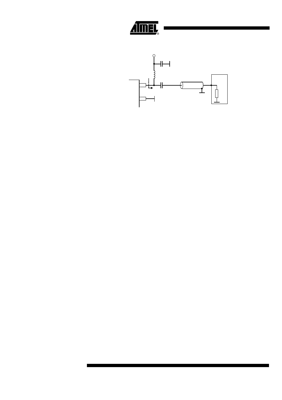
Figure 5.
Output Power Measurement
Application Circuit
For the supply-voltage blocking capacitor C
3
, a value of 68 nF/X7R is recommended
(see Figure 6 and Figure 7). C
1
and C
2
are used to match the loop antenna to the power
amplifier where C
1
typically is 22 pF/NP0 and C
2
is 10.8 pF/NP0 (18 pF + 27 pF in
series); for C
2
two capacitors in series should be used to achieve a better tolerance
value and to have the possibility to realize the Z
Load,opt
by using standard valued
capacitors.
C
1
forms together with the pins of PLL transmitter block and the PCB board wires a
series resonance loop that suppresses the 1
st
harmonic, thus, the position of C
1
on the
PCB is important. Normally the best suppression is achieved when C
1
is placed as close
as possible to the pins ANT1 and ANT2.
The loop antenna should not exceed a width of 1.5 mm, otherwise the Q-factor of the
loop antenna is too high.
L
1
(
[
50 nH to 100 nH) can be printed on PCB. C
4
should be selected so the XTO runs on
the load resonance frequency of the crystal. Normally, a value of 12 pF results for a
15 pF load-capacitance crystal.
~
~
ANT2
ANT1
Rin
Power
meter
C
1
= 1n
L
1
= 33n
C
2
= 2.2p
Z
Lopt
V
S
Z = 50
W
50
W