Timer 2 registers, Timer 2 control register (t2c), Timer 2 mode register 1 (t2m1) – Rainbow Electronics ATAR862-3 User Manual
Page 50: Atar862-3
50
ATAR862-3
4556B–4BMCU–02/03
Timer 2 Registers
Timer 2 has 6 control registers to configure the timer mode, the time interval, the input
clock and its output function. All registers are indirectly addressed using extended
addressing as described in section "Addressing Peripherals". The alternate functions of
the Ports BP41 or BP42 must be selected with the Port 4 control register P4CR, if one of
the Timer 2 modes require an input at T2I/BP41 or an output at T2O/BP42.
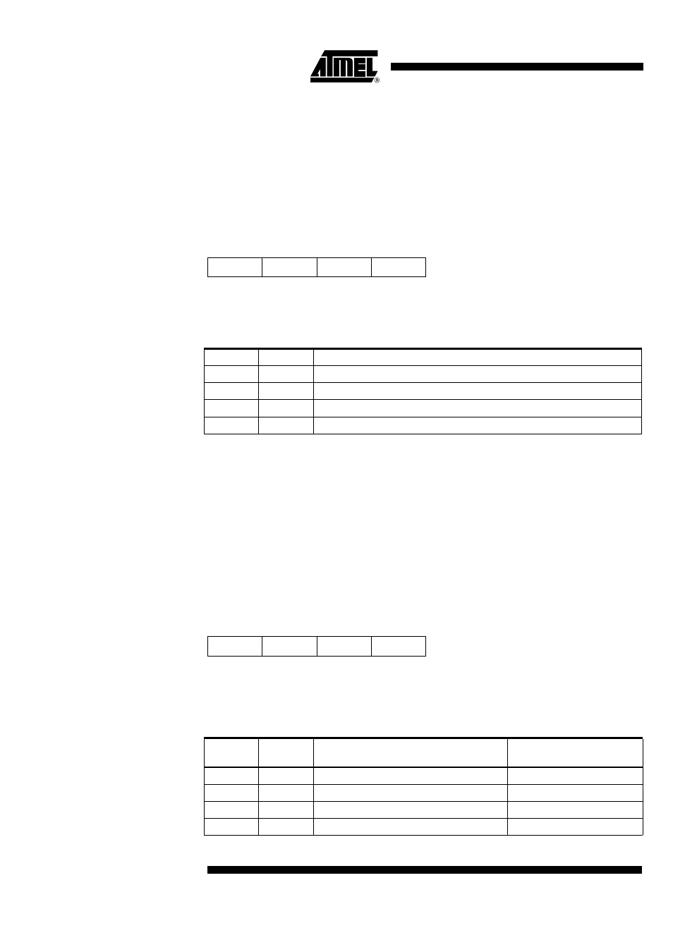
Timer 2 Control Register (T2C)
Address: "7"hex - Subaddress: "0"hex
Timer 2 Mode Register 1
(T2M1)
Address: "7"hex - Subaddress: "1"hex
Bit 3
Bit 2
Bit 1
Bit 0
T2CS1
T2CS0
T2TS
T2R
Reset value: 0000b
T2CS1
T
imer
2
C
lock
S
elect bit
1
T2CS0
T
imer
2
C
lock
S
elect bit
0
T2CS1
T2CS0
Input Clock (CL 2/1) of Counter Stage 2/1
0
0
System clock (SYSCL)
0
1
Output signal of Timer 1 (T1OUT)
1
0
Internal shift clock of SSI (SCL)
1
1
Output signal of Timer 3 (TOG3)
T2TS
T
imer
2
T
oggle with
S
tart
T2TS = 0, the output flip-flop of Timer 2 is not toggled with the timer start
T2TS = 1, the output flip-flop of Timer 2 is toggled when the timer is started with
T2R
T2R
T
imer
2
R
un
T2R = 0, Timer 2 stop and reset
T2R = 1, Timer 2 run
Bit 3
Bit 2
Bit 1
Bit 0
T2D1
T2D0
T2MS1
T2MS0
Reset value: 1111b
T2D1
T
imer
2
D
uty cycle bit
1
T2D0
T
imer
2
D
uty cycle bit
0
T2D1
T2D0
Function of Duty Cycle Generator
(DCG)
Additional Divider Effect
1
1
Bypassed (DCGO0)
/1
1
0
Duty cycle 1/1 (DCGO1)
/2
0
1
Duty cycle 1/2 (DCGO2)
/3
0
0
Duty cycle 1/3 (DCGO3)
/4