Rainbow Electronics BR24C21FV User Manual
Page 5
BR24C21 / BR24C21F / BR24C21FJ / BR24C21FV
Memory ICs
!
!
!
!
Circuit operation
The BR24C21, BR24C21F, BR24C21FJ and BR24C21FV operate in two modes, Transmit-Only Mode and Bi-directional
Mode. The devices operate in Transmit-Only Mode when they will power up. In this mode, the devices transmit data on
the SDA pin with the VCLK clock. This mode is continued by providing a valid high to low transition on the SCL pin.
The devices can be switched into Bi-directional Mode by providing a valid high to low transition on the SCL pin. They
begin to count the VCLK clock at once. If the VCLK counter reaches 128 clock without the command for Bi-directional
Mode, the device revert to Transmit-Only Mode. (Recovery function) If the devices are received the command for Bi-
directional Mode and respond with an Acknowledge before the VCLK counter reaches 128 clock, it is impossible to revert
to Transmit-Only Mode. (The way to switch Bi-directional Mode to Transmit-Only Mode is that the power down again.)
* When the power is on, the SCL pin set to V
CC
(High level).
(1) Transmit-Only Mode
•After the power is on, the BR24C21, BR24C21F, BR24C21FJ and BR24C21FV are in Transmit-Only Mode. In this
mode, the data can be output by providing the clock on the VCLK pin.
•When the power is on, the SCL pin set to V
CC
(High level).
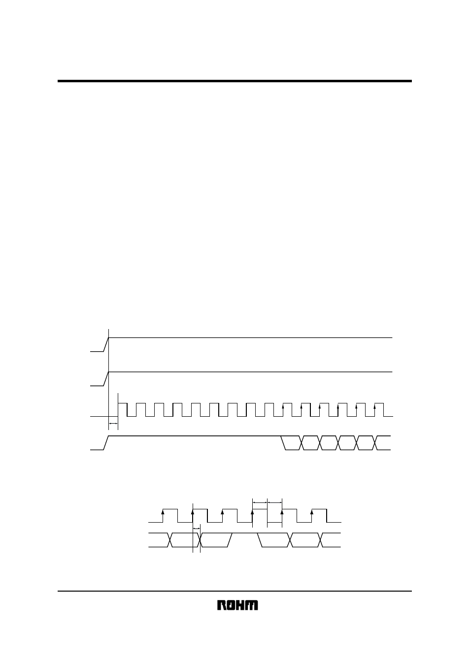
•The state of SDA is high-impedance during input of the first 9 clocks, and a data is output starting with the 10th rising
clock edge on VCLK. After the power is on, the output data is as follow
00h address data
→ 01h address data → 02h address data → …
The address is incremented by one with every 9 clock of VCLK. All address is output in this mode. When the counter
reaches the last address, the next output data is 00h address data.
•In the mode, the NULL bit (High data) is output between the address data and the next address data.
•The read operation in Transmit-Only Mode can be started after the power stabilized.
Fig.10 TRANSMIT-ONLY MODE
00h ADDRESS DATA
SDA
VCLK
SCL
V
CC
t
VPU
D3
D4
D5
D6
D7
1
9
10
Fig.11 NULL BIT
ADDRESS n
DATA
ADDRESS n+1
DATA
NULL BIT
DATA=1
SDA
VCLK
D1
D0
D7
D6
t
VPD
t
VHIGH
t
VLOW