General circuit description – Rainbow Electronics AT86RF230 User Manual
Page 5
5
AT86RF230
5131A-ZIGB-06/14/06
2. General Circuit Description
LNA
PPF
ADC
AGC
PA
Frequency
Synthesis
I
Q
FTN
AVREG
BATMON
SPI
Slave
Interface
TX power
control
TX Data
Limiter
5
RSSI
XOSC
Control Logic/
Configuration
Registers
CLKM
X
T
A
L
1
X
T
A
L
2
TRX Data
Buffer
TX BBP
RX BBP
BPF
IRQ
SEL
SCLK
MISO
MOSI
SLP_TR
RSTN
DCLK
RFP
RFN
Digital Domain
Analog Domain
DVREG
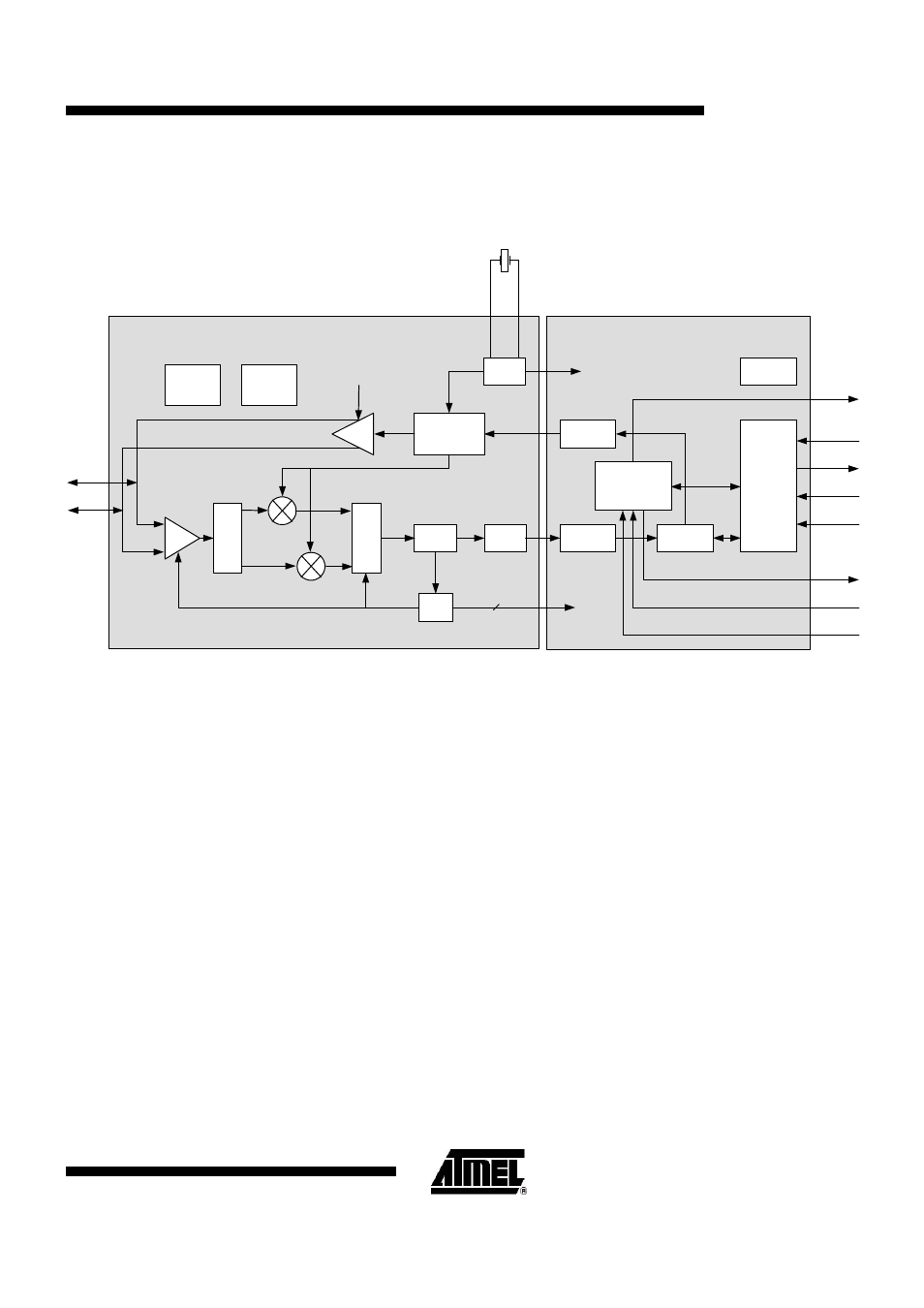
Figure 2-1.
Block Diagram of AT86RF230
This single-chip RF transceiver provides a complete radio interface between the antenna and the micro-controller.
It comprises the analog radio part, digital demodulation including time and frequency synchronization and data
buffering. The number of external components is minimized so that only the antenna, the crystal and four
decoupling capacitors are required. The bidirectional differential antenna pins are used in common for RX and TX,
so no external antenna switch is needed.
The transceiver block diagram is shown in Figure 2-1. The receiver path is based on a low-IF topology. The
channel filter consists of three single side-band active RC resonators forming a 2 MHz band-pass filter with a
Butterworth characteristic centered at 2 MHz. Two 1
st
-order high-pass filters were added to the signal path to
achieve capacitive coupling at the single side-band filter (SSBF) output to suppress DC offset and integrator
feedback at the limiter amplifier. The 3-stage limiter amplifier provides sufficient gain to overcome the DC offset of
the succeeding single channel ADC and generates a digital RSSI signal with 3 dB granularity. The low-IF signal is
sampled at 16 MHz with 1-bit resolution and applied to the digital signal processing part.
Direct VCO modulation is used to generate the transmit signal. The modulation scheme is offset-QPSK (O-QPSK)
with half-sine pulse shaping and 32-length block coding (spreading). This is equivalent to minimum shift keying
(MSK) when transforming the spreading code sequences appropriately. The modulation signal is applied to both
the VCO and the fractional-N PLL to ensure the coherent phase modulation required for demodulation as an O-
QPSK signal. The frequency-modulated LO signal is fed to the power amplifier.
Two on-chip low-dropout voltage regulators provide the analog and digital 1.8V supply. The SPI interface and the
control registers will retain their settings in SLEEP mode when the regulators are turned off. The RX and TX signal
processing paths are highly integrated and optimized for low power consumption.