Rainbow Electronics AT86RF230 User Manual
Page 15
15
AT86RF230
5131A-ZIGB-06/14/06
4.3.3.
State Transition Timing
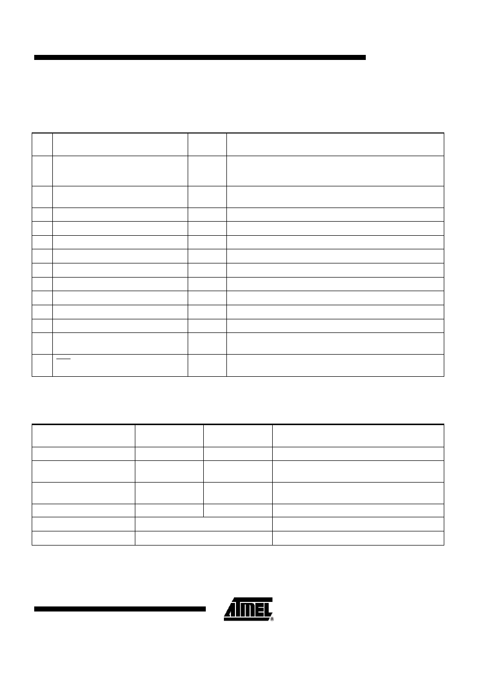
The transition numbers correspond to Figure 4-1 and do not include SPI access time if not otherwise stated. See
measurement setup in Figure 9-1.
No
Transition
Time [µ
µ
µ
µs]
(typical)
Comments
1
P_ON
→
TRX_OFF
1880
Internal power-on reset, including 1000 µs for controller access,
depends on external block capacitor at VDEC1 (1 µF nom) and
crystal oscillator setup (C
L
= 10 pf)
2
SLEEP
→
TRX_OFF
880
Depends on external block capacitor at VDEC1 (1 µF nom) and
crystal oscillator setup (C
L
= 10 pf)
3
TRX_OFF
→
SLEEP
35
35 cycles of 1 MHz clock assumed.
4
TRX_OFF
→
PLL_ON
180
Depends on external block capacitor at VDEC2 (1 µF nom).
5
PLL_ON
→
TRX_OFF
1
6
TRX_OFF
→
RX_ON
180
7
RX_ON
→
TRX_OFF
1
8
PLL_ON
→
RX_ON
1
9
RX_ON
→
PLL_ON
1
10
PLL_ON
→
BUSY_TX
16
Asserting SLP_TR pin
11
BUSY_TX
→
PLL_ON
32
12
All modes
→
TRX_OFF
1
Using TRX_CMD FORCE_TRX_OFF (see register 0x02), not
valid for SLEEP mode
13
0
RST =
→
TRX_OFF
120
Depends on external block capacitor at VDEC1 (1 µF nom), not
valid for P_ON mode
Table 4-1.
State Transition Timing
The state transition timing is calculated based on the timing of the single blocks shown in Figure 4-2. The worst
case values include maximum operating temperature, minimum supply voltage, and device parameter variations.
Block
Time [µ
µ
µ
µ
s]
(typical)
Time [µ
µ
µ
µ
s]
(worst case)
Comments
XOSC
500
1000
Depends on crystal Q factor and load capacitor.
DVREG
60
1000
Depends on external block capacitor at VDEC1
(CB3 = 1 µF nom., 10 µF worst case).
AVREG
60
1000
Depends on external block capacitor at VDEC2
(CB1 = 1 µF nom., 10 µF worst case).
PLL, initial
100
150
PLL, RX → TX
16
PLL, TX → RX
32
Table 4-2.
Block Timing