Rainbow Electronics AT84AD004 User Manual
Page 18
18
AT84AD004
5390A–BDC–06/04
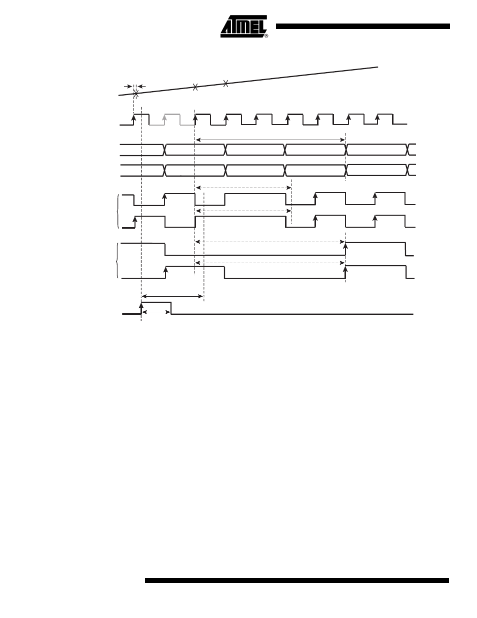
Figure 13. Data Ready Reset 1:2 DMUX Mode
Notes:
1. In 1:2 DMUX, Fs/2 mode:
The Data Ready Reset is taken into account only 2 ns after it is asserted. The output clock first completes its cycle (if the
reset occurs when it is low, it goes high only when its half cycle is complete; if the reset occurs when it is high, it remains
high) and then only, remains in reset state (frozen to a high level in 1:2 DMUX Fs/2 mode). The next rising edge of the input
clock after reset makes the output clock return to normal mode (after TDR).
2. In 1:2 DMUX, Fs/4 mode:
The Data Ready Reset is taken into account only 2 ns after it is asserted. The output clock first completes its cycle (if the
reset occurs when it is high, it goes low only when its half cycle is complete; if the reset occurs when it is low, it remains low)
and then only, remains in reset state (frozen to a low level in 1:2 DMUX Fs/4 mode). The next rising edge of the input clock
after reset makes the output clock return to normal mode (after TDR).
CLKI or
CLKQ
CLKOI or CLKOQ
(= CLKI/2)
DOIA[0:7] or
DOQA[0:7]
VIN
TA
N
N
DDRB
Pipeline Delay + TDO
N + 1
2 ns
DOIB[0:7] or
DOQB[0:7]
N + 1
CLKOI or CLKOQ
(= CLKI/4)
1 ns min
TDR
TDR
TDR + 2 cycles
TDR + 2 cycles
Clock in
Reset