Rainbow Electronics AT84AD004 User Manual
Page 11
11
AT84AD004
5390A–BDC–06/04
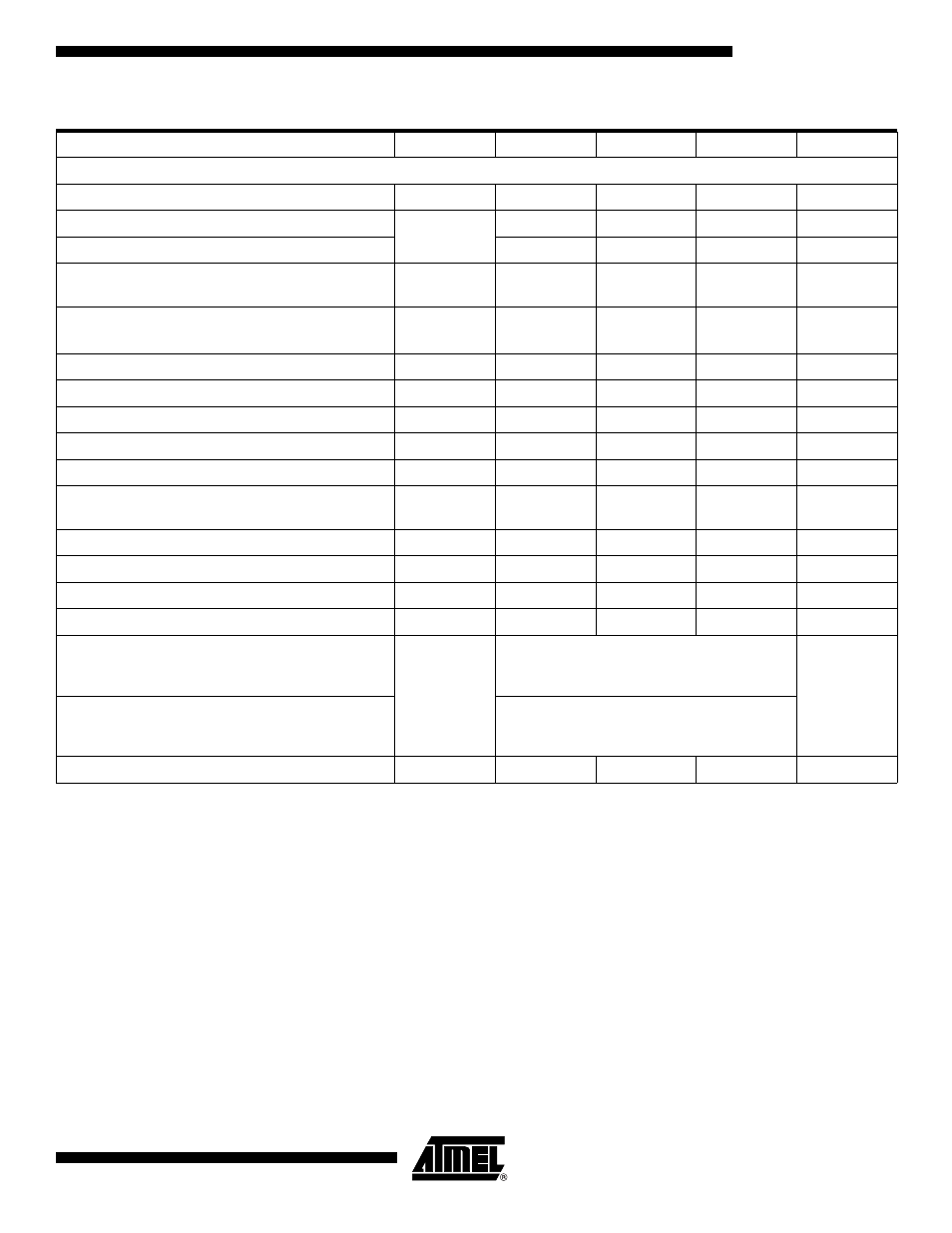
Table 5. Switching Performances
Parameter
Symbol
Min
Typ
Max
Unit
Switching Performance and Characteristics - See “Timing Diagrams” on page 12.
Maximum operating clock frequency
F
S
500
Msps
Minimum clock frequency (no transparent mode)
F
S
10
Msps
Minimum clock frequency (with transparent mode)
1
Ksps
Minimum clock pulse width [high]
(No transparent mode)
TC1
0.4
1
50
ns
Minimum clock pulse width [low]
(No transparent mode)
TC2
0.4
1
50
ns
Aperture delay: nominal mode with ISA & FiSDA
TA
1
ns
Aperture uncertainty
Jitter
0.4
ps (rms)
Data output delay between input clock and data
TDO
3.8
ns
Data Ready Output Delay
TDR
3
ns
Data Ready Reset to Data Ready
TRDR
2
ns
Data Output Delay with Data Ready
TD2
1/2 Fs
+Tdrda
ps
Data Ready (CLKO) Delay Adjust (140 ps steps)
Tdrda range
-560 to 420
ps
Output skew
50
100
ps
Output rise/fall time for DATA (20% - 80%)
TR/TF
300
350
500
ps
Output rise/fall time for DATA READY (20% - 80%)
TR/TF
300
350
500
ps
Data pipeline delay (nominal mode)
TPD
3 (port B)
3.5 (port A, 1:1 DMUX mode)
4 (port A, 1:2 DMUX mode)
Clock cycles
Data pipeline delay (nominal mode) in S/H
transparent mode
2.5 (port B)
3 (port A, 1:1 DMUX mode)
3.5 (port A, 1:2 DMUX mode)
DDRB recommended pulse width
1
ns